|
|
|
PDF DS28E04-100 Data sheet ( Hoja de datos )
| Número de pieza | DS28E04-100 | |
| Descripción | 4096-Bit Addressable 1-Wire EEPROM with PIO | |
| Fabricantes | Dallas Semiconducotr | |
| Logotipo | ||
Hay una vista previa y un enlace de descarga de DS28E04-100 (archivo pdf) en la parte inferior de esta página. Total 30 Páginas | ||
|
No Preview Available !
www.maxim-ic.com
GENERAL DESCRIPTION
The DS28E04-100 is a 4096-bit, 1-Wire® EEPROM
chip with seven address inputs. The address inputs
are directly mapped into the 1-Wire 64-bit Device ID
Number to easily enable the host system to identify
the physical location or functional association of the
DS28E04-100 in a multidevice 1-Wire network en-
vironment. The 4096-bit EEPROM array is configured
as 16 pages of 32 bytes with a 32 byte scratchpad to
perform write operations. EEPROM memory pages
can be individually write protected or put in EPROM-
emulation mode, where bits can only be changed
from a 1 to a 0 state. In addition to the memory, the
DS28E04-100 has two general-purpose I/O ports that
can be used for input or to generate level and/or
pulse outputs. Activity registers also capture port
activity for state change monitoring. The DS28E04-
100 communicates over the single-contact 1-Wire
bus. The communication follows the standard Dallas
Semiconductor 1-Wire protocol.
APPLICATIONS
· Autoconfiguration of Modular Systems such as
Central-Office Switches, Cellular Base Stations,
Access Products, Optical Network Units, and
PBXs
· Accessory/PCB Identification
TYPICAL OPERATING CIRCUIT
VCC
RPUP
PX.Y
µC
LED
IO VCC A6
POL
P1
P0
GND
A0
DS28E04 #1
IO VCC A6
POL
P1
P0
GND
A0
RST1 RST0 DS28E04 #7
DS28E04-100
4096-Bit Addressable 1-Wire EEPROM
with PIO
FEATURES
· 4096 bits of EEPROM Memory Partitioned into
16 Pages of 256 Bits
· Seven Address Inputs for Physical Location
Configuration
· Two General-Purpose PIO Pins with Pulse-
Generation Capability
§ Individual Memory Pages can be Permanently
Write-Protected or put in OTP EPROM-
Emulation Mode (“Write to 0”)
§ Communicates to Host with a Single Digital
Signal at 15.3kbps or 111kbps Using 1-Wire
Protocol
§ Parasitic or VCC Powered
§ Conditional Search Based on PIO Status or PIO
Activity
§ Switchpoint Hysteresis and Filtering to Optimize
Performance in the Presence of Noise
§ Reads and Writes Over a Wide 2.8V to 5.25V
Voltage Range from -40°C to +85°C
§ 16-Pin, 150-mil SO Package
ORDERING INFORMATION
PART
TEMP RANGE PIN-PACKAGE
DS28E04S-100
-40°C to +85°C 16 SO (150 mils)
DS28E04S-100/T&R -40°C to +85°C Tape-and-Reel
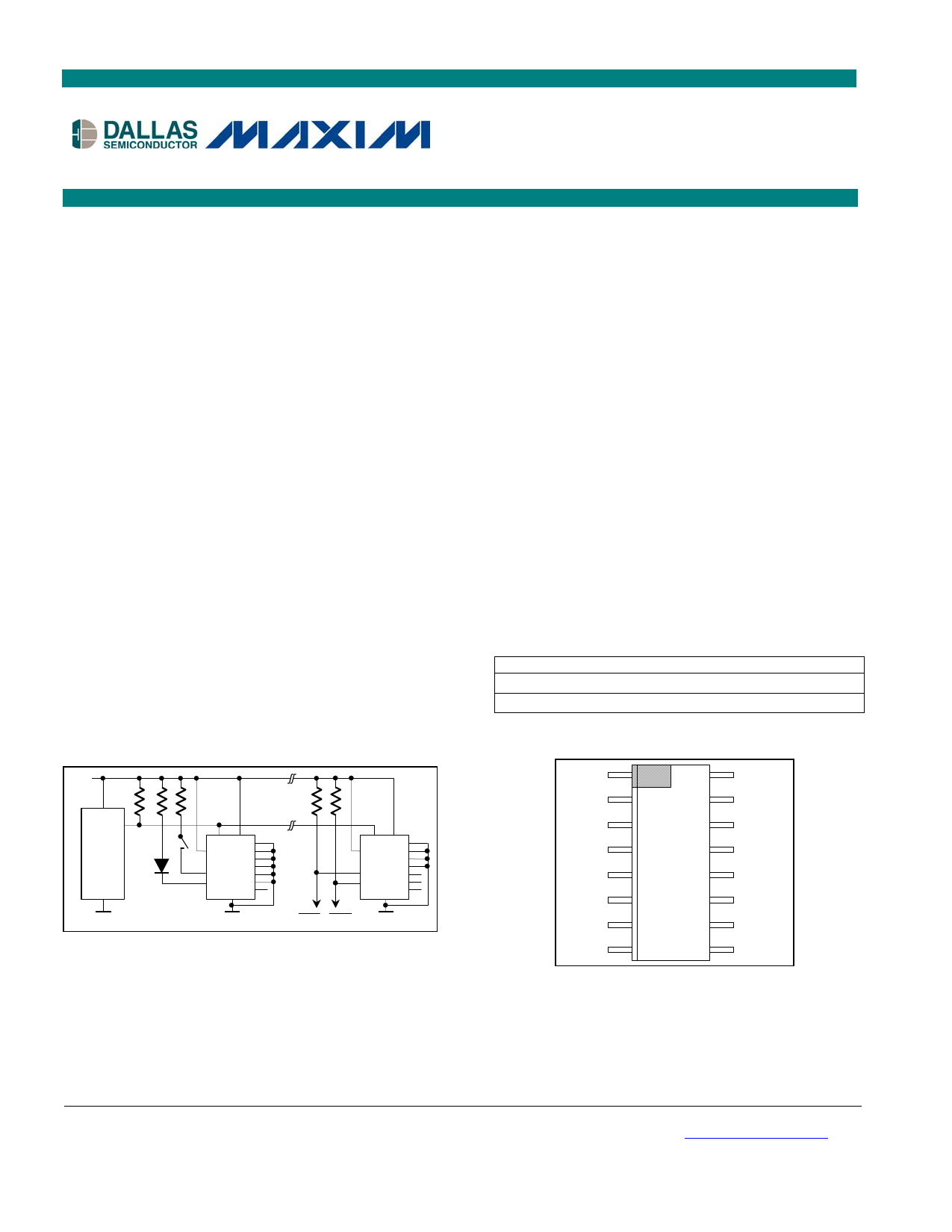
PIN CONFIGURATION
A3
A2
A1
A0
GND
N.C.
VCC
POL
1 16 IO
2 15 A4
3 14 A5
4 13 A6
5 12 GND
6 11 N.C.
7 10 P1
8 9 P0
SO (150 mils)
Commands, Registers, and Modes are capitalized for
clarity.
1-Wire is a registered trademark of Dallas Semiconductor Corp.
Note: Some revisions of this device may incorporate deviations from published specifications known as errata. Multiple revisions of any device
may be simultaneously available through various sales channels. For information about device errata, click here: www.maxim-ic.com/errata.
1 of 36
REV: 102704
1 page 
DS28E04-100: 4096-Bit 1-Wire Addressable EEPROM with PIO
OVERVIEW
The block diagram in Figure 1 shows the relationships between the major control and memory sections of the
DS28E04-100. The DS28E04-100 has five main data components: 1) 64-bit device ID number, 2) 32-byte
scratchpad, 3) sixteen 32-byte pages of EEPROM, 4) Special Function Register, and 5) PIO Control Registers. The
hierarchical structure of the 1-Wire protocol is shown in Figure 2. The bus master must first provide one of the eight
ROM Function Commands, 1) Read ROM, 2) Match ROM, 3) Search ROM, 4) Conditional Search ROM, 5) Skip
ROM, 6) Resume, 7) Overdrive-Skip ROM or 8) Overdrive-Match ROM. Upon completion of an Overdrive ROM
command byte executed at standard speed, the device enters Overdrive mode where all subsequent
communication occurs at a higher speed. The protocol required for these ROM function commands is described in
Figure 14. After a ROM function command is successfully executed, the memory/control functions become
accessible and the master may provide any one of the nine Memory/Control Function commands. The protocol for
these commands is described in Figure 9. All data is read and written least significant bit first.
Figure 1. Block Diagram
Internal VDD
VCC
1-Wire Network
IO
1-Wire
Function Control
P0
P1
POL
Memory
Function
Control Unit
PIO
Control Registers
Device ID
Number Register
A0
A6
CRC16
Generator
Data Memory
16 Pages of
32 Bytes Each
Special Function
Registers
32-Byte
Scratchpad
Internal VDD
5 of 36
5 Page 
DS28E04-100: 4096-Bit 1-Wire Addressable EEPROM with PIO
Conditional Search Channel Polarity Selection Register
ADDR b7 b6 b5 b4 b3 b2 b1 b0
0224h
0
0
0
0
0
0 SP1 SP0
The data in this register specifies the polarity of each selected PIO channel for the device to respond to the
conditional search command. This register can only be written through the Write Registers command. Within a PIO
channel, the data source may be either the channel's input pin or the channel's activity latch, as specified by the
PLS bit in the Control/Status register at address 0225h. This register is read/write. Each bit is associated with the
respective PIO channel as shown in Figure 7. Bits 2 to 7 have no function; they always read 0 and cannot be
changed to 1. This register is cleared to 00h at power-up.
Control/Status Register
ADDR b7 b6 b5 b4 b3 b2 b1 b0
0225h VCCP POL
0
0 PORL 0
CT PLS
The data in this register reports status information and further configures the device for conditional search. This
register can only be written through the Write Registers command. This register is read/write. The power-up state
of the PORL bit is "1". CT and PLS power up as "0". The functional assignments of the individual bits are explained
in the table below. Bits 2, 4, and 5 have no function; they always read 0 and cannot be set to 1.
Control/Status Register Details
BIT DESCRIPTION
BIT(S)
PLS: Pin or Activity
Latch Select
b0
CT: Conditional Search
Logical Term
b1
PORL: Power-On Reset
Latch
b3
POL: PIO Default
Polarity (Read-Only)
b6
VCCP: VCC Power
Status (Read-Only)
b7
DEFINITION
Selects either the PIO pins or the PIO activity latches as input for the
conditional search.
0: pin selected (default)
1: activity latch selected
Specifies whether the data of two channels needs to be OR’ed or
AND’ed to meet the qualifying condition for the device to respond to
a conditional search. If only a single channel is selected in the
channel selection mask (0223h) this bit is a don't care.
0: bitwise OR (default)
1: bitwise AND
Specifies whether the device has performed a power-on reset. This
bit can only be cleared to 0 by writing to the Control/Status Register.
As long as this bit is 1 the device will always respond to a Conditional
Search ROM sequence.
Reports the state of the POL pin. The state of the POL pin specifies
whether the PIO pins P0 and P1 power up high or low. The polarity
of a pulse generated at a PIO pin is the opposite of the pin's power-
up state.
0: PIO powers up 0
1: PIO powers up 1
For VCC-powered operation, the VCC pin needs to be connected to a
voltage source equal to VPUP.
0: VCC power not available
1: VCC-powered operation
11 of 36
11 Page | ||
| Páginas | Total 30 Páginas | |
| PDF Descargar | [ Datasheet DS28E04-100.PDF ] | |
Hoja de datos destacado
| Número de pieza | Descripción | Fabricantes |
| DS28E04-100 | 4096-Bit Addressable 1-Wire EEPROM with PIO | Dallas Semiconducotr |
| DS28E04-100 | 4096-Bit Addressable 1-Wire EEPROM with PIO | Dallas Semiconducotr |
| Número de pieza | Descripción | Fabricantes |
| SLA6805M | High Voltage 3 phase Motor Driver IC. |
Sanken |
| SDC1742 | 12- and 14-Bit Hybrid Synchro / Resolver-to-Digital Converters. |
Analog Devices |
|
DataSheet.es es una pagina web que funciona como un repositorio de manuales o hoja de datos de muchos de los productos más populares, |
| DataSheet.es | 2020 | Privacy Policy | Contacto | Buscar |