|
|
|
PDF CXA1619BS Data sheet ( Hoja de datos )
| Número de pieza | CXA1619BS | |
| Descripción | FM/AM Radio | |
| Fabricantes | Sony Corporation | |
| Logotipo | ||
1. CXA1619BS Hay una vista previa y un enlace de descarga de CXA1619BS (archivo pdf) en la parte inferior de esta página. Total 11 Páginas | ||
|
No Preview Available !
CXA1619BM/BS
FM/AM Radio
For the availability of this product, please contact the sales office.
Description
CXA1619BM/BS is a one-chip FM/AM radio IC
designed for radio-cassette tape recorders and
headphone tape recorders, and has the following
functions.
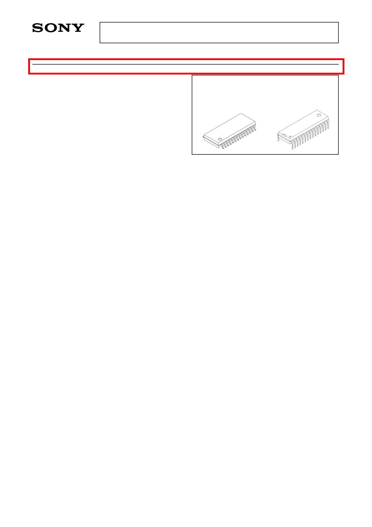
CXA1619BM
28 pin SOP (Plastic)
CXA1619BS
30 pin SDIP (Plastic)
Features
• Small number of peripheral components.
• Low current consumption (VCC=3 V)
For FM : ID=5.8 mA (Typ.)
For AM : ID=4.7 mA (Typ.)
• Built-in FM/AM select switch.
• Large output of AF amplifier.
EIAJ output=500 mW (Typ.) when
VCC=6 V, load impedance 8 Ω
Function
FM section
• RF amplifier, Mixer and OSC
(incorporating AFC variable capacitor).
• IF amplifier
• Quadrature detection
• Tuning LED driver
AM section
• RF amplifier, Mixer and OSC (with RF AGC)
• IF amplifier (with IF AGC)
• Detector
• Tuning LED driver
AF section
• Electronic volume control
Absolute Maximum Ratings (Ta=25 °C)
• Supply voltage
VCC 14 V
• Operating temperature Topr –10 to +60 °C
• Storage temperature Tstg –50 to +125 °C
• Allowable power dissipation
PD 700 mW
(CXA1619BM)
PD 1000 mW
(CXA1619BS)
Recommended Operating Conditions
Supply voltage
VCC 2 to 7.5 V
(CXA1619BM)
VCC 2 to 8.5 V
(CXA1619BS)
Structure
Bipolar monolithic IC
Sony reserves the right to change products and specifications without prior notice. This information does not convey any license by
any implication or otherwise under any patents or other right. Application circuits shown, if any, are typical examples illustrating the
operation of the devices. Sony cannot assume responsibility for any problems arising out of the use of these circuits.
—1—
E99214-TE
1 page 
CXA1619BM/BS
No. Symbol
19 (20) METER
20 (21) GND
21 (22) AFC/AGC
22 (23) AFC/AGC
23 (24) DET OUT
Voltage (V)
VCC=3 V VCC=6 V
FM AM FM AM
1.6 1.6 4.5 4.5
Equivalent circuit
1.25V
19
×3
N
GND
Description
Meter drive circuit
(For tuning indicator)
0000
1.25 1.49 1.25 1.49
22
1.25 1.25 1.25 1.25
1.25 1.0 1.25 1.0
33k 39k
23
AFC pin of W band.
During AM, it determines
time constant of AGC
AFC pin of J band.
21 During AM, it determines
time constant of AGC.
GND
Detection output pin
24 (25) AF IN
0000
11k
24
×4 ×4
82k
Power amplifier input pin
GND
RIPPLE
25 (26)
FILTER
2.71 2.71 5.4 5.4
25
VCC
17k
Ripple filter
73k
90k
26 (27) VCC
28
GND
(29, 30)
3.0 3.0 6.0 6.0
0000
Power supply pin
Power GND
∗ The pin voltage of pin 6 during AM, it is the same pin voltage of pin 22 (23) during J BAND and is the same
pin voltage of pin 21 (22) during W BAND.
—5—
5 Page 
Package Outline Unit : mm
CXA1619BM
28
28PIN SOP (PLASTIC)
+ 0.4
18.8 – 0.1
15
+ 0.4
2.3 – 0.15
0.15
+ 0.2
0.1 – 0.05
1
0.45 ± 0.1
14
1.27
+ 0.1
0.2 – 0.05
CXA1619BM/BS
CXA1619BS
0.24 M
SONY CODE
EIAJ CODE
JEDEC CODE
SOP-28P-L04
SOP028-P-0375
PACKAGE STRUCTURE
PACKAGE MATERIAL
LEAD TREATMENT
LEAD MATERIAL
PACKAGE MASS
EPOXY RESIN
SOLDER PLATING
42/COPPER ALLOY
0.7g
30PIN SDIP (PLASTIC)
+ 0.4
26.9 – 0.1
30 16
1 15
1.778
0° to 15°
0.5 ± 0.1
0.9 ± 0.15
SONY CODE
EIAJ CODE
JEDEC CODE
SDIP-30P-01
SDIP030-P-0400
Two kinds of package surface:
1.All mat surface type.
2.All mirror surface type.
PACKAGE STRUCTURE
MOLDING COMPOUND EPOXY RESIN
LEAD TREATMENT
SOLDER/PALLADIUM
PLATING
LEAD MATERIAL
COPPER ALLOY
PACKAGE MASS
1.8g
NOTE : PALLADIUM PLATING
This product uses S-PdPPF (Sony Spec.-Palladium Pre-Plated Lead Frame).
—11—
11 Page | ||
| Páginas | Total 11 Páginas | |
| PDF Descargar | [ Datasheet CXA1619BS.PDF ] | |
Hoja de datos destacado
| Número de pieza | Descripción | Fabricantes |
| CXA1619BM | FM/AM Radio | Sony Corporation |
| CXA1619BS | FM/AM Radio | Sony Corporation |
| Número de pieza | Descripción | Fabricantes |
| SLA6805M | High Voltage 3 phase Motor Driver IC. |
Sanken |
| SDC1742 | 12- and 14-Bit Hybrid Synchro / Resolver-to-Digital Converters. |
Analog Devices |
|
DataSheet.es es una pagina web que funciona como un repositorio de manuales o hoja de datos de muchos de los productos más populares, |
| DataSheet.es | 2020 | Privacy Policy | Contacto | Buscar |