|
|
|
PDF LTC3206 Data sheet ( Hoja de datos )
| Número de pieza | LTC3206 | |
| Descripción | I2C Multidisplay LED Controller | |
| Fabricantes | Linear Technology | |
| Logotipo | ||
Hay una vista previa y un enlace de descarga de LTC3206 (archivo pdf) en la parte inferior de esta página. Total 16 Páginas | ||
|
No Preview Available !
FEATURES
■ Step-Up/Direct-Connect Fractional Charge Pump
Provides Up to 92% Efficiency
■ Up to 400mA Continuous Output Current
■ Independent Current and Dimming Control for
1-6 LED MAIN, 1-4 LED SUB and RGB LED Displays
■ LED Currents Programmable Using 2-Wire I2C™
Serial Interface
■ 1% LED Current Matching
■ Low Noise Constant Frequency Operation*
■ Minimal Component Count
■ Automatic Soft-Start Limits Inrush Current
■ 16 Exponentially Spaced Dimming States Provides
128:1 Brightness Range for MAIN and SUB Displays
■ Up to 4096 Color Combinations for RGB Display
■ Low Operating Current: IVIN = 180µA
■ Tiny, Low Profile 24-Lead (4mm × 4mm × 0.75mm)
QFN Package
U
APPLICATIO S
■ Cellular Phones
■ Wireless PDAs
■ Multidisplay Handheld Devices
, LTC and LT are registered trademarks of Linear Technology Corporation.
I2C is a trademark of Philips Electronics N.V.
* U.S. Patent 6,411,531
LTC3206
I2C Multidisplay
LED Controller
DESCRIPTIO
The LTC®3206 is a highly integrated multidisplay LED con-
troller. The part contains a high efficiency, low noise frac-
tional step-up/direct-connect charge pump to provide
power for both main and sub white LED displays plus an
RGB color LED display. The LTC3206 requires only four
small ceramic capacitors plus two resistors to form a
complete 3-display LED power supply and current
controller.
Maximum currents for the main/sub displays and RGB
display are set independently. Current for each LED is
controlled with an internal current source. Dimming and
ON/OFF control for all displays is achieved via a 2-wire
serial interface. Two auxiliary LED pins can be individually
assigned to either the MAIN or SUB displays. 16 individual
dimming states exist for both the MAIN and SUB displays.
Each of the RED, GREEN and BLUE LEDs have 16 dimming
states as well, resulting in up to 4096 color combinations.
The LTC3206 charge pump optimizes efficiency based on
VIN and LED forward voltage conditions. The part powers
up in direct-connect mode and automatically switches to
1.5x step-up mode once any enabled LED current source
begins to enter dropout. Internal circuitry prevents inrush
current and excess input noise during start-up and mode
switching. The LTC3206 is available in a 24-lead (4mm ×
4mm) QFN package.
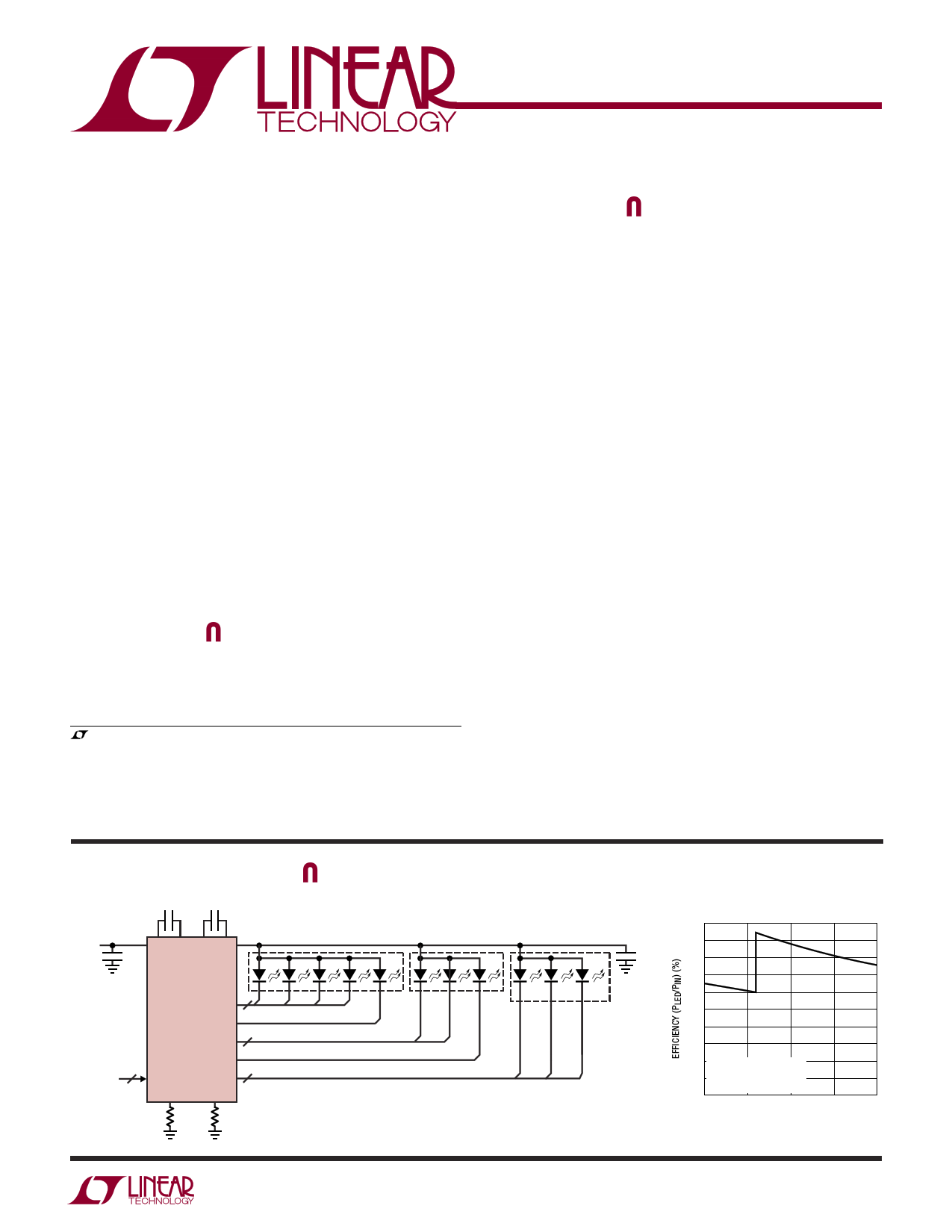
TYPICAL APPLICATIO
2.2µF
2.2µF
VIN
2.7V TO
4.5V
VIN
2.2µF
CPO
LTC3206
I2C SERIAL 2
INTERFACE
4
MAIN1-4
AUX 1
2
SUB1-2
AUX 2
SERIAL PORT RGB
IRGB
IMS
3
MAIN DISPLAY
SUB DISPLAY
RGB ILLUMINATOR
RED GREEN BLUE
3206 TA01a
5-LED Main Display Efficiency
vs Input Voltage
2.2µF
100
90
80
70
60
50
40
30
20 FIVE LEDs AT 15mA/LED
10 (TYP VF AT 15mA = 3.2V)
TA = 25°C
0
3.0 3.3 3.6
3.9
INPUT VOLTAGE (V)
4.2
3206 TA01b
3206f
1
1 page 
LTC3206
PI FU CTIO S
SUB1, SUB2 (Pins 1, 2): Current Source Outputs for the
SUB Display White LEDs. The current for the SUB display
is controlled by the resistor on the IMS pin.The LEDs on the
SUB display can be set to exponentially increasing bright-
ness levels from 0.78% to 100% of full-scale. See Table 1.
C1+, C1–, C2+, C2– (Pins 5, 4, 6, 3): Charge Pump Flying
Capacitor Pins. A 2.2µF X7R or X5R ceramic capacitor
should be connected from C1+ to C1– and another from
C2+ to C2–.
DVCC (Pin 7): This pin sets the logic reference level of the
SDA, SCL and ENRGB/S pins.
SDA (Pin 8): Input Data for the I2C Serial Port. Serial data
is shifted in one bit per clock to control the LTC3206 (see
Figures 3 and 4). The logic level for SDA is referenced to
DVCC.
SCL (Pin 9): Clock Input for the I2C Serial Port (see Figures
3 and 4). The logic level for SCL is referenced to DVCC.
ENRGB/S (Pin 10): This pin is used to enable and disable
either the RED, GREEN and BLUE current sources or the
SUB display depending on which is programmed to re-
spond via the I2C port. Once ENRGB/S is brought high, the
LTC3206 illuminates the RGB or SUB display with the
color combination or intensity that was previously pro-
grammed via the I2C port. The logic level for ENRGB/S is
referenced to DVCC.
IMS (Pin 11): This pin controls the maximum amount of
LED current in both the MAIN and SUB LED displays. The
IMS pin servos to 0.6V when there is a resistor to ground.
The full scale (100%) currents in the MAIN and SUB
display LEDs will be 400 times the current at the IMS pin.
IRGB (Pin 12): This pin controls the amount of LED current
at the RED, GREEN and BLUE LED pins. The IRGB pin
servos to 0.6V when there is a resistor to ground. The
current in the RED, GREEN and BLUE LEDs will be 400
times the current at the IRGB pin when programmed to full
scale.
SGND (Pin 13): Ground for the control logic. This pin
should be connected directly to a low impedance ground
plane.
CPO (Pin 14): Output of the Charge Pump. This output
should be used to power white, blue and “true” green
LEDs. Red LEDs can be powered from VIN or CPO. An X5R
or X7R low impedance (ceramic) 2.2µF charge storage
capacitor is required on CPO.
VIN (Pin 15): Supply Voltage for the Charge Pump. The VIN
pin should be connected directly to the battery and by-
passed with a 2.2µF X5R or X7R ceramic capacitor.
RED, GREEN, BLUE (Pins 16, 17, 18): Current Source
Outputs for the RGB Illuminator LEDs. The currents for the
RGB LEDs are controlled by the resistor on the IRGB pin.
The RGB LEDs can independently be set to any duty cycle
from 0/15 through 15/15 under software control giving a
total of 16 shades per LED and 4096 colors for the
illuminator. See Table 1. The RGB LEDs are modulated at
1/240 the speed of the charge pump oscillator (approxi-
mately 4kHz).
MAIN1-MAIN4 (Pins 22, 21, 20, 19): Current Source
Outputs for the Main Display White LEDs. The current for
the main display is controlled by the resistor on the IMS
pin. The LEDs on the MAIN display can be set to 16
exponentially increasing brightness steps from 0.78% to
100% of full scale. See Table 1.
AUX1, AUX2 (Pins 23, 24): Current source outputs for the
auxiliary white LEDs. The auxiliary current sources can be
individually assigned to be either MAIN display or SUB
display LEDs via the I2C serial port. When either AUX1 and/
or AUX2 are assigned to the MAIN display they will have
the same power setting as the other MAIN LEDs. Likewise,
when either AUX1 and/or AUX2 are assigned to the SUB
display they will have the same power setting as the other
SUB LEDs. The currents for the AUX1 and AUX2 pins are
controlled by the resistor on the IMS pin.
PGND (Pin 25, Exposed Pad): Power Ground for the
Charge Pump. This pin should be connected directly to a
low impedance ground plane.
3206f
5
5 Page 
LTC3206
APPLICATIO S I FOR ATIO
The RED, GREEN and BLUE pins can also enable the
charge pump, however, since they each have individual
disable control they can be left floating or grounded if
unused.
RGB Illuminator Brightness Control
The RED, GREEN and BLUE LEDs can be individually set
to have a linear duty cycle ranging from 0/15 (off) to
15/15 (full on) with 1/15 increments in between. The
combination of 16 possible brightness levels gives the
RGB indicator LED a total of 4096 colors. Table 1 indicates
the decoding of the RED, GREEN and BLUE LEDs.
The full-scale currents in the RED, GREEN and BLUE LEDs
are controlled by the current at the IRGB pin in a similar
manner to those in the MAIN, SUB and AUX LEDs. The
IRGB pin also servos to 0.6V and the RGB LED currents are
a precise multiple of the IRGB current. The DC value of the
RGB display LED currents will follow the relationship:
IRED,GREEN,BLUE
=
400
0.6V
RRGB
where RRGB is the value of the resistor at the IRGB pin.
The average value of the current in the RED, GREEN and
BLUE LEDs will be:
AVG
(IRED,GREEN,BLUE)
=
400
•
D
15
•
0.6V
RRGB
where D is the decimal equivalent of the 4-bit digital code
programmed for the given LED(0 to 15). Table 1 summa-
rizes the RED, GREEN and BLUE LED power settings.
The RED, GREEN and BLUE LEDs are pulse width modu-
lated at a frequency of 1/240 of the frequency of the charge
pump oscillator or about 4kHz.
ENRGB/S Pin
The ENRGB/S pin can be used to enable or disable the
LTC3206 without re-accessing the I2C port. This might be
useful to indicate an incoming phone call without waking
the microcontroller. ENRGB/S can be software pro-
grammed as an independent control for either the RGB
display or the SUB display. Control bit A2 in the serial port
(see Figure 3 and Table 3) determines which display
ENRGB/S controls. When bit A2 is 0, the ENRGB/S pin
controls the RGB display. If it is set to 1, ENRGB/S controls
the SUB display.
To use the ENRGB/S pin, the I2C port must first be
configured to the desired setting. For example, if ENRGB/S
will be used to control the SUB display, then a non-zero
code must reside in the C3-C0 nibble of the I2C port and bit
A2 must be set to 1 (see Table 1). Now when ENRGB/S is
high (DVCC), the SUB display will be on with the C3-C0
setting. When ENRGB/S is low, the SUB display will be off.
If no other displays are programmed to be on, the entire
chip will be in shutdown.
Likewise, if ENRGB/S will be used to enable the RGB
display, then a non-zero code must reside in one of the
RED, GREEN or BLUE nibbles of the serial port (A4-A7 or
B0-B7), and bit A2 must be 0. Now when ENRGB/S is high
(DVCC), the RGB display will light with the programmed
color. When ENRGB/S is low, the RGB display will be off.
If no other displays are programmed to be on, the entire
chip will be in shutdown.
If bit A2 is set to 1 (SUB display control), then ENRGB/S
will have no effect on the RGB display. Likewise, if bit A2
is set to 0 (RGB display control), then ENRGB/S will have
no effect on the SUB display.
If the ENRGB/S pin is not used, it should be connected to
DVCC. It should not be grounded or left floating.
VIN, CPO Capacitor Selection
The style and value of capacitors used with the LTC3206
determine several important parameters such as regulator
control-loop stability, output ripple and charge pump
strength. To reduce noise and ripple, it is recommended
that low equivalent series resistance (ESR) multilayer
ceramic capacitors be used on both VIN and CPO. Tanta-
lum and aluminum capacitors are not recommended be-
cause of their high ESR. The value of the capacitor on CPO
directly controls the amount of output ripple for a given
load current. Increasing the size of this capacitor will
reduce the output ripple. The peak-to-peak output ripple is
approximately given by the expression:
VRIPPLEP-P
≅
ICPO
3fOSC • CCPO
3206f
11
11 Page | ||
| Páginas | Total 16 Páginas | |
| PDF Descargar | [ Datasheet LTC3206.PDF ] | |
Hoja de datos destacado
| Número de pieza | Descripción | Fabricantes |
| LTC3200 | Regulated Charge Pump DC/DC Converters | Linear Technology |
| LTC3200-5 | Regulated Charge Pump DC/DC Converters | Linear Technology |
| LTC3201 | 100mA Ultralow Noise Charge Pump Led Supply | Linear Technology Corporation |
| LTC3202 | Low Noise/ High Efficiency Charge Pump for White LEDs | Linear Technology |
| Número de pieza | Descripción | Fabricantes |
| SLA6805M | High Voltage 3 phase Motor Driver IC. |
Sanken |
| SDC1742 | 12- and 14-Bit Hybrid Synchro / Resolver-to-Digital Converters. |
Analog Devices |
|
DataSheet.es es una pagina web que funciona como un repositorio de manuales o hoja de datos de muchos de los productos más populares, |
| DataSheet.es | 2020 | Privacy Policy | Contacto | Buscar |