|
|
|
PDF LTC3202 Data sheet ( Hoja de datos )
| Número de pieza | LTC3202 | |
| Descripción | Low Noise/ High Efficiency Charge Pump for White LEDs | |
| Fabricantes | Linear Technology | |
| Logotipo | ||
Hay una vista previa y un enlace de descarga de LTC3202 (archivo pdf) en la parte inferior de esta página. Total 13 Páginas | ||
|
No Preview Available !
LTC3202
Low Noise, High Efficiency
Charge Pump for White LEDs
FEATURES
s Low Noise Constant Frequency Operation
s 25% Less Input Current Than Doubler Charge Pump
s High Output Current: Up To 125mA
s Small Application Circuit
s Regulated Output Voltage or Current
s Automatic Soft-Start
s VIN Range: 2.7V to 4.5V
s No Inductors
s 1.5MHz Switching Frequency
s ICC < 1µA in Shutdown
s Available in 10-Pin MSOP and 3mm × 3mm
DFN Packages U
APPLICATIO S
s White LED Backlighting
s Programmable Boost Current Source
DESCRIPTIO
The LTC®3202 is a low noise, constant frequency charge
pump DC/DC converter that uses fractional conversion to
increase efficiency in white LED applications. The part can
be used to produce a regulated voltage or current of up to
125mA from a 2.7V to 4.5V input. Low external parts count
(two flying capacitors and two small bypass capacitors at
VIN and VOUT) make the LTC3202 ideally suited for small,
battery-powered applications.
An internal 2-bit DAC allows LED current to be adjusted for
LED brightness control. The LTC3202 also has thermal
shutdown protection and can survive a continuous short-
circuit from VOUT to GND. Built-in soft-start circuitry
prevents excessive inrush current during start-up. High
switching frequency enables the use of small external
capacitors. A low current shutdown feature disconnects
the load from VIN and reduces quiescent current to less
than1µA.
The LTC3202 is available in the 10-pin MSOP and 3mm ×
3mm DFN packages.
, LTC and LT are registered trademarks of Linear Technology Corporation.
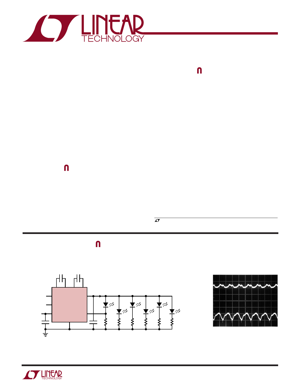
TYPICAL APPLICATIO
Programmable White LED Power Supply
C2 C3
1µF 1µF
8 79 6
C1+
10 D0
CURRENT
C1–
C2+
C2–
0mA TO 125mA
3 TOTAL CURRENT
VOUT
PROGRAMMING 1 D1 LTC3202
VIN
3V TO 4.5V
C1
1µF
4 VIN
2
FB
GND
5, 11
C4
1µF
36Ω
36Ω
36Ω
36Ω
36Ω 36Ω
C1, C2, C3, C4 = MURATA GRM 39X5R105K6.3 OR TAIYO YUDEN JMK107BJ105MA
3202 TA01
Input and Output Ripple
VIN
(AC COUPLED)
20mV/DIV
VOUT
(AC COUPLED)
20mV/DIV
VIN = 3.6V
500ns/DIV
CIN = COUT = 1µF
IOUT = 60mA
3202 G09
3202fa
1
1 page 
SI PLIFIED BLOCK DIAGRA
LTC3202
FB 2
VIN 4
VOUT 3
2-BIT
DAC
SOFT-START AND
SHUTDOWN
CONTROL
1.5MHz
OSCILLATOR
10 D0
1 D1
8 C1+
7 C1–
9 C2+
6 C2–
5, 11 GND
3202 BD
3202fa
5
5 Page 
LTC3202
PACKAGE DESCRIPTIO
MS Package
10-Lead Plastic MSOP
(Reference LTC DWG # 05-08-1661)
0.889 ± 0.127
(.035 ± .005)
3.00 ± 0.102
(.118 ± .004)
(NOTE 3)
10 9 8 7 6
5.23
(.206)
MIN
3.20 – 3.45
(.126 – .136)
0.305 ± 0.038
(.0120 ± .0015)
TYP
0.50
(.0197)
BSC
RECOMMENDED SOLDER PAD LAYOUT
0.254
(.010)
GAUGE PLANE
DETAIL “A”
0° – 6° TYP
0.53 ± 0.152
(.021 ± .006)
DETAIL “A”
0.18
(.007)
NOTE:
1. DIMENSIONS IN MILLIMETER/(INCH)
2. DRAWING NOT TO SCALE
3. DIMENSION DOES NOT INCLUDE MOLD FLASH, PROTRUSIONS OR GATE BURRS.
MOLD FLASH, PROTRUSIONS OR GATE BURRS SHALL NOT EXCEED 0.152mm (.006") PER SIDE
4. DIMENSION DOES NOT INCLUDE INTERLEAD FLASH OR PROTRUSIONS.
INTERLEAD FLASH OR PROTRUSIONS SHALL NOT EXCEED 0.152mm (.006") PER SIDE
5. LEAD COPLANARITY (BOTTOM OF LEADS AFTER FORMING) SHALL BE 0.102mm (.004") MAX
SEATING
PLANE
4.90 ± 0.152
(.193 ± .006)
12345
1.10
(.043)
MAX
0.17 – 0.27
(.007 – .011)
TYP
0.50
(.0197)
BSC
0.497 ± 0.076
(.0196 ± .003)
REF
3.00 ± 0.102
(.118 ± .004)
(NOTE 4)
0.86
(.034)
REF
0.127 ± 0.076
(.005 ± .003)
MSOP (MS) 0603
DD Package
10-Lead Plastic DFN (3mm × 3mm)
(Reference LTC DWG # 05-08-1699)
0.55 ±0.05
R = 0.115
TYP
6
0.38 ± 0.10
10
3.35 ±0.05
1.65 ±0.05
2.25 ±0.05 (2 SIDES)
PIN 1
PACKAGE TOP MARK
OUTLINE
0.25 ± 0.05
0.50
BSC
2.38 ±0.05
(2 SIDES)
0.200 REF
RECOMMENDED SOLDER PAD PITCH AND DIMENSIONS
NOTE:
1. DRAWING TO BE MADE A JEDEC PACKAGE OUTLINE M0-229 VARIATION OF (WEED-2)
2. ALL DIMENSIONS ARE IN MILLIMETERS
3. DIMENSIONS OF EXPOSED PAD ON BOTTOM OF PACKAGE DO NOT INCLUDE
MOLD FLASH. MOLD FLASH, IF PRESENT, SHALL NOT EXCEED 0.15mm ON ANY SIDE
4. EXPOSED PAD SHALL BE SOLDER PLATED
3.00 ±0.10
(4 SIDES)
1.65 ± 0.10
(2 SIDES)
0.75 ±0.05
0.00 – 0.05
(DD10) DFN 0103
51
0.25 ± 0.05
0.50 BSC
2.38 ±0.10
(2 SIDES)
BOTTOM VIEW—EXPOSED PAD
Information furnished by Linear Technology Corporation is believed to be accurate and reliable.
However, no responsibility is assumed for its use. Linear Technology Corporation makes no represen-
tation that the interconnection of its circuits as described herein will not infringe on existing patent rights.
3202fa
11
11 Page | ||
| Páginas | Total 13 Páginas | |
| PDF Descargar | [ Datasheet LTC3202.PDF ] | |
Hoja de datos destacado
| Número de pieza | Descripción | Fabricantes |
| LTC3200 | Regulated Charge Pump DC/DC Converters | Linear Technology |
| LTC3200-5 | Regulated Charge Pump DC/DC Converters | Linear Technology |
| LTC3201 | 100mA Ultralow Noise Charge Pump Led Supply | Linear Technology Corporation |
| LTC3202 | Low Noise/ High Efficiency Charge Pump for White LEDs | Linear Technology |
| Número de pieza | Descripción | Fabricantes |
| SLA6805M | High Voltage 3 phase Motor Driver IC. |
Sanken |
| SDC1742 | 12- and 14-Bit Hybrid Synchro / Resolver-to-Digital Converters. |
Analog Devices |
|
DataSheet.es es una pagina web que funciona como un repositorio de manuales o hoja de datos de muchos de los productos más populares, |
| DataSheet.es | 2020 | Privacy Policy | Contacto | Buscar |