|
|
|
PDF AN80M19RSP Data sheet ( Hoja de datos )
| Número de pieza | AN80M19RSP | |
| Descripción | 5-pin/ low dropout voltage regulator with standby function (500 mA type) | |
| Fabricantes | Panasonic Semiconductor | |
| Logotipo | ||
Hay una vista previa y un enlace de descarga de AN80M19RSP (archivo pdf) en la parte inferior de esta página. Total 29 Páginas | ||
|
No Preview Available !
Voltage Regulators
AN80MxxRSP Series
5-pin, low dropout voltage regulator with standby function (500 mA type)
I Overview
The AN80MxxRSP series is a 0.5 A, low dropout
voltage regulator IC with standby function, featuring low
current consumption and low noise.
I Features
• Standby consumption current: max. 3 µA
• Dropout voltage: 0.25 V
• Output voltage accuracy: ±3%
• 5-pin surface mounting package
• Ripple rejection ratio: 30 dB (f = 500 kHz)
• Output voltage: 1.8 V, 1.9 V, 2.0 V, 2.1 V, 2.2 V, 2.5 V,
2.7 V, 2.8 V, 2.9 V, 3.0 V, 3.1 V, 3.2 V,
3.3 V, 3.4 V, 3.5 V, 3.6 V, 4.8 V, 4.9 V,
5.0 V, 5.1 V, 5.2 V, 5.3 V
I Applications
• General use power supply
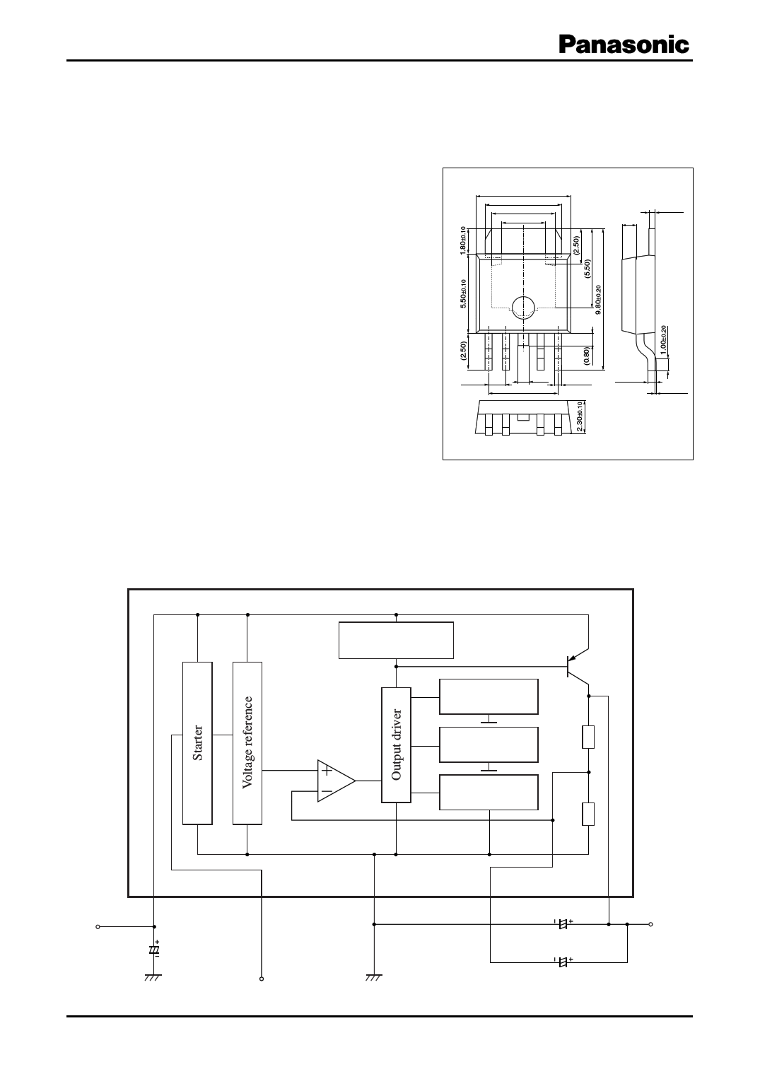
I Block Diagram
6.50±0.10
5.40±0.10
(4.35)
(3.00)
Unit: mm
1.00±0.10
0.50±0.10
3
1
1.27±0.10
2 45
(0.75)
5.08±0.10
0.50±0.10
0.50±0.10
0.10±0.10
SP-5SU
Note) The package of this product will be changed
to lead-free type (SP-5SUA). See the new pack-
age dimensions section later of this datasheet.
Input short-circuit
protection
Output stage
VREF
Error amplifier
Overcurrent
limitter
Inrush current
protection
Thermal
protection
R1
R2
1
VIN
CIN 3.3 µF
2
Cont.
Publication date: November 2001
3
(Fin)
SFF00009CEB
45
COUT 33 µF
CNR 1 µF
VOUT
1
1 page 
AN80MxxRSP Series
I Electrical Characteristics at Ta = 25°C (continued)
• AN80M19RSP (1.9 V type)
Unless otherwise specially provided, shorten each test time (within 10 ms) so that the test is conducted under the condition that
the drift due to the temperature increase in the chip junction part can be neglected. CIN = 3.3 µF, CNR = Open, COUT = 33 µF
Parameter
Symbol
Conditions
Min Typ Max Unit
Output voltage
VOUT VIN = 2.9 V, IOUT = 250 mA
1.843 1.9 1.957
Line regulation
REGIN VIN = 2.9 V → 14.0 V, IOUT = 250 mA 19
Load regulation
REGLOA VIN = 2.9 V, IOUT = 0 mA → 500 mA 38
Peak output current
IPEAK
VIN = 2.9 V, The output current value
when VOUT decreases by 5% from
its value at IOUT = 250 mA.
600
900
Bias current under no load
IBIAS VIN = 2.9 V, IOUT = 0 mA
1.1 3.0
Bias current fluctuation to input ∆IBIAS(IN) VIN = 2.9 V → 14.0 V, IOUT = 250 mA −5
5
Bias current fluctuation to load ∆IBIAS(LOA) VIN = 2.9 V, IOUT = 0 mA → 500 mA 25
Standby consumption current
ISTB VIN = 14.0 V, VCONT = 0 V
3.0
Bias current before starting regulation IRUSH VIN = 1.805 V, IOUT = 0 A
5
Control terminal current
ICONT
VIN = 2.9 V, IOUT = 250 mA
VCONT = 1.8 V
30
Ripple rejection ratio 1
RR1 VIN = 3.9 V±1 V, f = 120 Hz
IOUT = 100 mA
58.4
Minimum input/
output voltage difference 1
VDIF(min)1 VIN = 2.0 V, IOUT = 250 mA
0.25 0.45
V
mV
mV
mA
mA
mA
mA
µA
mA
µA
dB
V
Minimum input/
output voltage difference 2
VDIF(min)2 VIN = 2.1 V, IOUT = 500 mA
0.8 V
Control terminal threshold high voltage VCONTH VIN = 2.9 V
Control terminal threshold low voltage VCONTL VIN = 2.9 V
1.45 1.80
0.50 0.70
V
V
• Design reference data
Note) The following values are typical and not guaranteed values.
Parameter
Symbol
Conditions
Min Typ Max Unit
Ripple rejection ratio 2
Output noise voltage
Output voltage temperature
coefficient
RR2 VIN = 3.9 V±1 V, f = 500 kHz
IOUT = 100 mA
30 dB
VNO 10 Hz ≤ f ≤ 100 kHz, IOUT = 100 mA 40 µV[rms]
VIN = 2.9 V, CNR = 1 µF
dVOUT VIN = 2.9 V, IOUT = 5 mA
dTa −30°C ≤ Ta ≤ +125°C
±40 ppm/°C
Output short-circuit current
Overheat protection operating
temperature
IOSHORT VIN = 14.0 V, VOUT = GND
TjTH VIN = 2.9 V, IOUT = 5 mA
300 mA
150 °C
SFF00009CEB
5
5 Page 
AN80MxxRSP Series
I Electrical Characteristics at Ta = 25°C (continued)
• AN80M28RSP (2.8 V type)
Unless otherwise specially provided, shorten each test time (within 10 ms) so that the test is conducted under the condition that
the drift due to the temperature increase in the chip junction part can be neglected. CIN = 3.3 µF, CNR = Open, COUT = 33 µF
Parameter
Symbol
Conditions
Min Typ Max Unit
Output voltage
VOUT VIN = 3.8 V, IOUT = 250 mA
2.716 2.8 2.884
Line regulation
REGIN VIN = 3.8 V → 14.0 V, IOUT = 250 mA 28
Load regulation
REGLOA VIN = 3.8 V, IOUT = 0 mA → 500 mA 56
Peak output current
IPEAK
VIN = 3.8 V, The output current value
when VOUT decreases by 5% from
its value at IOUT = 250 mA.
600
900
Bias current under no load
IBIAS VIN = 3.8 V, IOUT = 0 mA
1.1 3.0
Bias current fluctuation to input ∆IBIAS(IN) VIN = 3.8 V → 14.0 V, IOUT = 250 mA −5
5
Bias current fluctuation to load ∆IBIAS(LOA) VIN = 3.8 V, IOUT = 0 mA → 500 mA 25
Standby consumption current
ISTB VIN = 14.0 V, VCONT = 0 V
3.0
Bias current before starting regulation IRUSH VIN = 2.660 V, IOUT = 0 A
5
Control terminal current
ICONT
VIN = 3.8 V, IOUT = 250 mA
VCONT = 1.8 V
30
Ripple rejection ratio 1
RR1 VIN = 4.8 V±1 V, f = 120 Hz
IOUT = 100 mA
55.0
Minimum input/
output voltage difference 1
VDIF(min)1 VIN = 2.9 V, IOUT = 250 mA
0.25 0.45
V
mV
mV
mA
mA
mA
mA
µA
mA
µA
dB
V
Minimum input/
output voltage difference 2
VDIF(min)2 VIN = 3.0 V, IOUT = 500 mA
0.8 V
Control terminal threshold high voltage VCONTH VIN = 3.8 V
Control terminal threshold low voltage VCONTL VIN = 3.8 V
1.45 1.80
0.50 0.70
V
V
• Design reference data
Note) The following values are typical and not guaranteed values.
Parameter
Symbol
Conditions
Min Typ Max Unit
Ripple rejection ratio 2
Output noise voltage
Output voltage temperature
coefficient
RR2 VIN = 4.8 V±1 V, f = 500 kHz
IOUT = 100 mA
30 dB
VNO 10 Hz ≤ f ≤ 100 kHz, IOUT = 100 mA 40 µV[rms]
VIN = 3.8 V, CNR = 1 µF
dVOUT VIN = 3.8 V, IOUT = 5 mA
dTa −30°C ≤ Ta ≤ +125°C
±40 ppm/°C
Output short-circuit current
Overheat protection operating
temperature
IOSHORT VIN = 14.0 V, VOUT = GND
TjTH VIN = 3.8 V, IOUT = 5 mA
300 mA
150 °C
SFF00009CEB
11
11 Page | ||
| Páginas | Total 29 Páginas | |
| PDF Descargar | [ Datasheet AN80M19RSP.PDF ] | |
Hoja de datos destacado
| Número de pieza | Descripción | Fabricantes |
| AN80M19RSP | 5-pin/ low dropout voltage regulator with standby function (500 mA type) | Panasonic Semiconductor |
| Número de pieza | Descripción | Fabricantes |
| SLA6805M | High Voltage 3 phase Motor Driver IC. |
Sanken |
| SDC1742 | 12- and 14-Bit Hybrid Synchro / Resolver-to-Digital Converters. |
Analog Devices |
|
DataSheet.es es una pagina web que funciona como un repositorio de manuales o hoja de datos de muchos de los productos más populares, |
| DataSheet.es | 2020 | Privacy Policy | Contacto | Buscar |