|
|
|
PDF AN7703F Data sheet ( Hoja de datos )
| Número de pieza | AN7703F | |
| Descripción | Low-dropout three-pin voltage regulator 1.2-A type | |
| Fabricantes | Panasonic Semiconductor | |
| Logotipo | ||
Hay una vista previa y un enlace de descarga de AN7703F (archivo pdf) en la parte inferior de esta página. Total 21 Páginas | ||
|
No Preview Available !
Voltage Regulators
AN7700, AN7700F, AN7700SP Series
Low-dropout three-pin voltage regulator 1.2-A type
s Overview
The AN7700, AN7700F, and AN7700SP series are
stabilized constant-voltage power supplies with small dif-
ference between I/O voltages (0.5 V typ.). They are suit-
able for low-voltage, battery-driven equipment, and home
appliances and industrial equipment with great fluctua-
tion of the supply voltage.
The output voltage ranges:
For AN7700, AN7700F
3 V, 4 V, 5 V, 6 V, 7 V, 8 V, 9 V, 10 V, 12 V, 15 V,
18 V, 20 V, and 24 V
For AN7700SP
3.3 V, 3.5 V, 5 V, 6 V, 7 V, 8 V, 9 V, 10 V, 12 V,
and 15 V
s Features
• Minimum I/O voltage difference: 0.5 V (typ.)
• On-chip overcurrent limiter
• On-chip thermal protection circuit
• On-chip inrush current protection circuit at the time of
input voltage start-up
• On-chip input short-circuit protection circuit
(When the input pin is short-circuited to the ground, the
circuit between pins 1 and 3 is shut down to prevent
current flow.)
s Applications
• Power supply equipment
AN7700 series
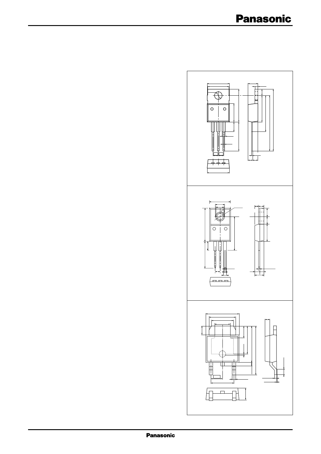
(10.35)
10.0±0.3
φ3.7±0.1
Unit: mm
4.5±0.2
1.4±0.1
1.4
+0.15
–0.05
0.8
+0.15
–0.05
2.54 2.54
0.45
+0.2
–0.0
(2.0) (2.5)
10.5±0.3
TO-220 Package (HSIP003-P-0000)
AN7700F series
Unit: mm
10.5±0.3
(4.3)
φ5.3 3.1±0.1
2.77±0.3
(1.73)
2.54
12
(0.4)
0.8±0.2
1.4±0.2
3
2.0
±0.25
0.4+–00..015
2.5±0.25
4.5±0.3
TO-220F Package (HSIP003-P-0000A)
AN7700SP series
6.50±0.10
5.30±0.10
4.35±0.20
3.00±0.20
Unit: mm
1.00±0.20
2.30
4.60±0.10
0.75±0.10
0.55±0.15
0.10±0.05
123
U-type Package
1
1 page 
Voltage Regulators
AN7700, AN7700F, AN7700SP Series
s Electrical Characteristics at Ta = 25°C (continued)
• AN77033SP (3.3-V type)
Parameter
Symbol
Conditions
Min Typ Max Unit
Output voltage
VOUT VIN = 4.3 V, IOUT = 500 mA,
Tj = 25°C
3.20 3.30 3.40
Line regulation
REGIN VIN = 4.3 V to 14.3 V,
IOUT = 500 mA, Tj = 25°C
3 35
Load regulation
REGLOA VIN = 4.3 V,
15 70
IOUT = 0 mA to 1 200 mA, Tj = 25°C
Input dependency of bias current
∆IBias(IN) VIN = 4.3 V to 14.3 V,
IOUT = 500 mA, Tj = 25°C
1 10
Load depndency of bias current ∆IBias(LOA) VIN = 4.3 V,
10 50
IOUT = 0 mA to 1 200 mA, Tj = 25°C
V
mV
mV
mA
mA
Bias current at no load
Bias current
before the regulation starts
IBias VIN = 4.3 V, IOUT = 0 mA
Irush VIN = 3.0 V, IOUT = 0 mA
2.6 5.0 mA
3
5 mA
Minimum I/O voltage difference 1 VDIF(min)1 VIN = 3.7 V, IOUT = 500 mA,
Tj = 25°C
Minimum I/O voltage difference 2 VDIF(min)2 VIN = 3.7 V, IOUT = 1 200 mA,
Tj = 25°C
Peak output current 1 *
IO(Peak)1 VIN = 4.3 V, Tj = 25 °C
Ripple rejection ratio
RR VIN = 4.3 V to 8.0 V,
IOUT = 100 mA, f = 120 Hz
0.4 0.6 V
0.5 1.0 V
1.2 1.8 2.4
53 74
A
dB
Note) *: This current exceeds PD(max) because it is a parameter during abnormal (overcurrent) operation. However, normally,
it shall conform to the derating curve ( s Characteristic curve chart PD Ta ).
• Design reference data
Note) The characteristics listed below are theoretical values based on the IC design and are not guaranteed.
Parameter
Symbol
Conditions
Min Typ Max
Peak output current 2 *
Peak output current 3 *
Output short-circuit current
IO(Peak)2 VIN = 13.3 V, Tj = 25°C
IO(Peak)3 VIN = 18.3 V, Tj = 25°C
IO(Short) VIN = 30 V, Tj = 25°C
The load is shorted.
1.5
1.0
10
Unit
A
A
mA
Thermal protection operating
temperature
Tj(TH) VIN = 4.3 V
150 °C
Output voltage temperature
coefficient
a VIN = 4.3 V, Tj = 25°C to 125°C
−40 ppm/°C
Note) *: This current exceeds PD(max) because it is a parameter during abnormal (overcurrent) operation. However, normally,
it shall conform to the derating curve ( s Characteristic curve chart PD Ta ).
5
5 Page 
Voltage Regulators
AN7700, AN7700F, AN7700SP Series
s Electrical Characteristics at Ta = 25°C (continued)
• AN7708/F/SP (8-V type)
Parameter
Symbol
Conditions
Min Typ Max Unit
Output voltage
VOUT VIN = 9 V, IOUT = 500 mA,
Tj = 25°C
7.76 8.00 8.24
Line regulation
REGIN VIN = 9 V to 19 V, IOUT = 500 mA, 8 80
Tj = 25°C
Load regulation
REGLOA VIN = 9 V, IOUT = 0 mA to 1 200 mA,
Tj = 25°C
40 160
Input dependency of bias current ∆IBias(IN) VIN = 9 V to 19 V, IOUT = 500 mA, 1 10
Tj = 25°C
Load dependency of bias current ∆IBias(LOA) VIN = 9 V, IOUT = 0 mA to 1 200 mA, 10 50
Tj = 25°C
Bias current at no load
IBias VIN = 9 V, IOUT = 0 mA
2.6 5.0
Bias current
before the regulation starts
Irush VIN = 7.2 V, IOUT = 0 mA
3
5
V
mV
mV
mA
mA
mA
mA
Minimum I/O voltage difference 1 VDIF(min)1 VIN = 7.2 V, IOUT = 500 mA,
Tj = 25°C
Minimum I/O voltage difference 2 VDIF(min)2 VIN = 7.2 V, IOUT = 1 200 mA,
Tj = 25°C
Peak output current 1 *
Peak output current 2 *
(Excluding the SP type)
IO(Peak)1 VIN = 9 V, Tj = 25°C
IO(Peak)2 VIN = 18 V, Tj = 25°C
Peak output current 3 *
(Excluding the SP type)
IO(Peak)3 VIN = 23 V, Tj = 25°C
0.4 0.6 V
0.5 1.0 V
1.2 1.8 2.4
1.0 1.5 2.0
A
A
0.5 1.0 1.5 A
Ripple rejection ratio
RR VIN = 9 V to 11 V, IOUT = 100 mA, 46 66 dB
f = 120 Hz
Note) *: This current exceeds PD(max) because it is a parameter during abnormal (overcurrent) operation. However, normally,
it shall conform to the derating curve ( s Characteristic curve chart PD Ta ).
• Design reference data
Note) The characteristics listed below are theoretical values based on the IC design and are not guaranteed.
Parameter
Symbol
Conditions
Min Typ Max Unit
Peak output current 2 *
(Only for the SP type)
IO(Peak)2 VIN = 18 V, Tj = 25°C
1.5 A
Peak output current 3 *
(Only for the SP type)
IO(Peak)3 VIN = 23 V, Tj = 25°C
1.0 A
Output short-circuit current
IO(Short) VIN = 30 V, Tj = 25°C
The load is shorted.
10 mA
Thermal protection operating
temperature
Tj(TH) VIN = 9 V
150 °C
Output voltage temperature
coefficient
a VIN = 9 V, Tj = 25°C to 125°C
−40 ppm/°C
Note) *: This current exceeds PD(max) because it is a parameter during abnormal (overcurrent) operation. However, normally,
it shall conform to the derating curve ( s Characteristic curve chart PD Ta ).
11
11 Page | ||
| Páginas | Total 21 Páginas | |
| PDF Descargar | [ Datasheet AN7703F.PDF ] | |
Hoja de datos destacado
| Número de pieza | Descripción | Fabricantes |
| AN7703 | Low-dropout three-pin voltage regulator 1.2-A type | Panasonic Semiconductor |
| AN77033SP | Low-dropout three-pin voltage regulator 1.2-A type | Panasonic Semiconductor |
| AN77035SP | Low-dropout three-pin voltage regulator 1.2-A type | Panasonic Semiconductor |
| AN7703F | Low-dropout three-pin voltage regulator 1.2-A type | Panasonic Semiconductor |
| Número de pieza | Descripción | Fabricantes |
| SLA6805M | High Voltage 3 phase Motor Driver IC. |
Sanken |
| SDC1742 | 12- and 14-Bit Hybrid Synchro / Resolver-to-Digital Converters. |
Analog Devices |
|
DataSheet.es es una pagina web que funciona como un repositorio de manuales o hoja de datos de muchos de los productos más populares, |
| DataSheet.es | 2020 | Privacy Policy | Contacto | Buscar |