|
|
|
PDF HV400MJ Data sheet ( Hoja de datos )
| Número de pieza | HV400MJ | |
| Descripción | High Current MOSFET Driver | |
| Fabricantes | Intersil Corporation | |
| Logotipo | ||
Hay una vista previa y un enlace de descarga de HV400MJ (archivo pdf) en la parte inferior de esta página. Total 11 Páginas | ||
|
No Preview Available !
HV400MJ/883
August 1997
High Current MOSFET Driver
Features
Description
• This Circuit is Processed in Accordance to MIL-STD-
883 and is Fully Conformant Under the Provisions of
Paragraph 1.2.1.
• Fast Fall Times . . . . . . . . . . . . . . . . . . .16ns at 10,000pF
• No Supply Current in Quiescent State
• Peak Source Current . . . . . . . . . . . . . . . . . . . . . . . . . .6A
• Peak Sink Current . . . . . . . . . . . . . . . . . . . . . . . . . . .30A
• High Frequency Operation . . . . . . . . . . . . . . . . . 300kHz
Applications
• Switch Mode Power Supplies
• DC/DC Converters
• Motor Controllers
• Uninterruptable Power Supplies
Ordering Information
PART NUMBER
HV400MJ/883
TEMP.
RANGE (oC)
PACKAGE
-55 to 125 8 Ld SBDIP
PKG.
NO.
D8.3
The HV400MJ/883 is a single monolithic, non-inverting high
current driver designed to drive large capacitive loads at high
slew rates. The device is optimized for driving single or paral-
lel connected N-Channel power MOSFETs with total gate
charge from 5nC to >1000nC. It features two output stages
pinned out separately allowing independent control of the
MOSFET gate rise and fall times. The current sourcing output
stage is an NPN capable of 6A. An SCR provides over 30A of
current sinking. The HV400MJ/883 achieves rise and fall
times of 54ns and 16ns respectively driving a 10,000pF load.
Special features are included in this part to provide a simple,
high speed gate drive circuit for power MOSFETs. The
HV400MJ/883 requires no quiescent supply current, how-
ever, the input current is approximately 15mA while in the
high state. With the internal current steering diodes (Pin 7)
and an external capacitor, both the timing and MOSFET gate
power come from the same pulse transformer; no special
external supply is required for high side switches. No high
voltage diode is required to charge the bootstrap capacitor.
The HV400MJ/883 in combination with the MOSFET and
pulse transformer makes an isolated power switch building
block for applications such as high side switches, secondary
side regulation and synchronous rectification. The
HV400MJ/883 is also suitable for driving IGBTs, MCTs,
BJTs and small GTOs.
The HV400MJ/883 is a type of buffer; it does not have input
logic level switching threshold voltages. This single stage
design achieves propagation delays of 20ns. The output
NPN begins to source current when the voltage on Pin 2 is
approximately 2V more positive than the voltage at Pin 8.
The output SCR switches on when the input Pin 2 is 1V
more negative than the voltage at Pins 3/6. Due to the use of
the SCR for current sinking, once the output switches low,
the input must not go high again until all the internal SCR
charge has dissipated, 0.5µs - 1.5µs later.
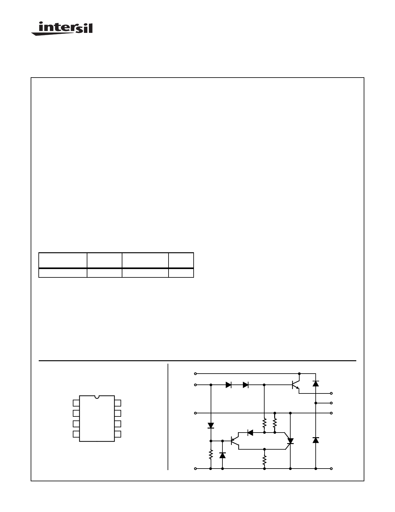
Pinout
HV400MJ/883 (SBDIP)
TOP VIEW
Schematic
PIN 1
PIN 2
V+ SUPPLY 1
INPUT 2
SINK OUTPUT 3
GND 4
8 SOURCE OUTPUT
7 DIODES
6 SINK OUTPUT
5 GND
PIN 3
D4
D3 D2
R4
Q2 D8
Q1
R2
SCR
D1
PIN 8
PIN 7
PIN 6
D7
R3
PIN 4
D6
R1
PIN 5
CAUTION: These devices are sensitive to electrostatic discharge; follow proper IC Handling Procedures.
http://www.intersil.com or 407-727-9207 | Copyright © Intersil Corporation 1999
1
File Number 3584.2
1 page 
HV400MJ/883
Switching Diagram and Test Circuit
INPUT
0V
VOUT
OUTPUT
10%
tDR tr
10%
90%
90%
tDF tf
90%
10%
10%
tOR
FIGURE 1.
+V
C1
330µF
50V
R1 100 1W
1N914
7
2
1
8
C2
1.0µF
50V
15V
GND
INPUT
50Ω SOURCE
(RISE AND FALL TIMES <10ns)
4
3 AND 6
CL
0.01µF
CHIP
CAP
FIGURE 2.
5
RL
100K
OUTPUT
12.8V
0.9V
5
5 Page 
HV400MJ/883
Ceramic Dual-In-Line Metal Seal Packages (SBDIP)
-A- -D-
E
-B-
bbb S C A - B S D S
c1 LEAD FINISH
BASE
METAL
(c)
b1
MM
(b)
SECTION A-A
BASE
PLANE
SEATING
PLANE
D
S1
b2
b
AA
e
ccc M C A - B S D S
S2 Q
-C- A
L
eA
eA/2
c
aaa M C A - B S D S
NOTES:
1. Index area: A notch or a pin one identification mark shall be locat-
ed adjacent to pin one and shall be located within the shaded
area shown. The manufacturer’s identification shall not be used
as a pin one identification mark.
2. The maximum limits of lead dimensions b and c or M shall be
measured at the centroid of the finished lead surfaces, when
solder dip or tin plate lead finish is applied.
3. Dimensions b1 and c1 apply to lead base metal only. Dimension
M applies to lead plating and finish thickness.
4. Corner leads (1, N, N/2, and N/2+1) may be configured with a
partial lead paddle. For this configuration dimension b3 replaces
dimension b2.
5. Dimension Q shall be measured from the seating plane to the
base plane.
6. Measure dimension S1 at all four corners.
7. Measure dimension S2 from the top of the ceramic body to the
nearest metallization or lead.
8. N is the maximum number of terminal positions.
9. Braze fillets shall be concave.
10. Dimensioning and tolerancing per ANSI Y14.5M - 1982.
11. Controlling dimension: INCH.
D8.3 MIL-STD-1835 CDIP2-T8 (D-4, CONFIGURATION C)
8 LEAD CERAMIC DUAL-IN-LINE METAL SEAL PACKAGE
INCHES
MILLIMETERS
SYMBOL MIN MAX MIN MAX NOTES
A
- 0.200 - 5.08
-
b
0.014
0.026
0.36
0.66
2
b1
0.014
0.023
0.36
0.58
3
b2
0.045
0.065
1.14
1.65
-
b3
0.023
0.045
0.58
1.14
4
c
0.008
0.018
0.20
0.46
2
c1
0.008
0.015
0.20
0.38
3
D
- 0.405 - 10.29
-
E
0.220
0.310
5.59
7.87
-
e 0.100 BSC
2.54 BSC
-
eA 0.300 BSC
7.62 BSC
-
eA/2
0.150 BSC
3.81 BSC
-
L
0.125
0.200
3.18
5.08
-
Q
0.015
0.060
0.38
1.52
5
S1 0.005 - 0.13 - 6
S2 0.005 - 0.13
-
α 90o 105o 90o 105o
aaa - 0.015 - 0.38
7
-
-
bbb
- 0.030 - 0.76
-
ccc
- 0.010 - 0.25
-
M
-
0.0015
-
0.038
2
N8
88
Rev. 0 4/94
All Intersil semiconductor products are manufactured, assembled and tested under ISO9000 quality systems certification.
Intersil products are sold by description only. Intersil Corporation reserves the right to make changes in circuit design and/or specifications at any time without
notice. Accordingly, the reader is cautioned to verify that data sheets are current before placing orders. Information furnished by Intersil is believed to be accurate
and reliable. However, no responsibility is assumed by Intersil or its subsidiaries for its use; nor for any infringements of patents or other rights of third parties which
may result from its use. No license is granted by implication or otherwise under any patent or patent rights of Intersil or its subsidiaries.
For information regarding Intersil Corporation and its products, see web site http://www.intersil.com
Sales Office Headquarters
NORTH AMERICA
Intersil Corporation
P. O. Box 883, Mail Stop 53-204
Melbourne, FL 32902
TEL: (407) 724-7000
FAX: (407) 724-7240
EUROPE
Intersil SA
Mercure Center
100, Rue de la Fusee
1130 Brussels, Belgium
TEL: (32) 2.724.2111
FAX: (32) 2.724.22.05
ASIA
Intersil (Taiwan) Ltd.
Taiwan Limited
7F-6, No. 101 Fu Hsing North Road
Taipei, Taiwan
Republic of China
TEL: (886) 2 2716 9310
FAX: (886) 2 2715 3029
11
11 Page | ||
| Páginas | Total 11 Páginas | |
| PDF Descargar | [ Datasheet HV400MJ.PDF ] | |
Hoja de datos destacado
| Número de pieza | Descripción | Fabricantes |
| HV400MJ | High Current MOSFET Driver | Intersil Corporation |
| HV400MJ883 | High Current MOSFET Driver | Intersil Corporation |
| Número de pieza | Descripción | Fabricantes |
| SLA6805M | High Voltage 3 phase Motor Driver IC. |
Sanken |
| SDC1742 | 12- and 14-Bit Hybrid Synchro / Resolver-to-Digital Converters. |
Analog Devices |
|
DataSheet.es es una pagina web que funciona como un repositorio de manuales o hoja de datos de muchos de los productos más populares, |
| DataSheet.es | 2020 | Privacy Policy | Contacto | Buscar |