|
|
|
PDF HV3922DJ Data sheet ( Hoja de datos )
| Número de pieza | HV3922DJ | |
| Descripción | High Voltage PIN Diode Driver | |
| Fabricantes | Supertex Inc | |
| Logotipo | ||
Hay una vista previa y un enlace de descarga de HV3922DJ (archivo pdf) en la parte inferior de esta página. Total 5 Páginas | ||
|
No Preview Available !
HV3922
High Voltage PIN Diode Driver
Ordering Information
Device
Package
20 Pin Ceramic DIP 28 Pin Ceramic J-Lead
HV3922
HV3922C
HV3922DJ
Features
❏ Processed with HVCMOS® technology
❏ 5V CMOS logic – low power dissipation
❏ DMOS output voltage up to 220V
❏ Low power level shifting – 5V to 220V
❏ Source current 1.7mA
❏ Output fault detection
❏ Latched data output
Absolute Maximum Ratings
Supply Voltage, VCC
Logic Input Voltage
-0.5V to +7.0V
-0.3V to VCC + 0.3V
Supply Voltage VLL
Supply Voltage VPP
Max Power Dissipation
-5.0V
+230V
0.8W
Junction Temperature
+150 °C
Storage Temperature Range
-65 °C to +150 °C
Operating Temperature Range
-55 °C to +125 °C
Lead Soldering Temperature for 10 Seconds
+300 °C
General Description
The HV3922 is a monolithic high-voltage quad-output driver that
is designed to be used in conjunction with the Supertex
VN2222NC*, a separate N-channel DMOS FET quad array,
whose device characterics are briefly described below. Together,
these devices per-form a 220V push-pull function that is espe-
cially suited for driving PIN diodes in applications such as fre-
quency-hopping radios, microwave communication systems and
phased array radar.
Used as a microwave or RF switch, the HV3922 has 4 high-
voltage P-channel outputs: PD0, PD1, PD2 and PD3. Additional
controls are Chip Select (CS) and Output Enable (OE) functions.
The HV3922 also has an output fault detection function that
protects the outputs from damage by putting them into a high
impedance state when a short is detected. The HV3922 provides
4 low-voltage outputs—DRV0, DRV1, DRV2 and DRV3—that drive
the gates of the 4 N-channel FETs in the VN2222NC device. See
the diagram below for an example of the push-pull output struc-
ture that these two devices provide.
For detailed electrical characteristics of the VN2222NC, please
see the data sheet in Chapter 8. Currently, the HV3922 is
available in through-hole and surface-mount ceramic packages
that are suitable for military applications, while the VN2222NC is
offered in ceramic quad and discrete packages (VN2224N2 and
VN2224N3). For commercial product availability, please consult
the factory.
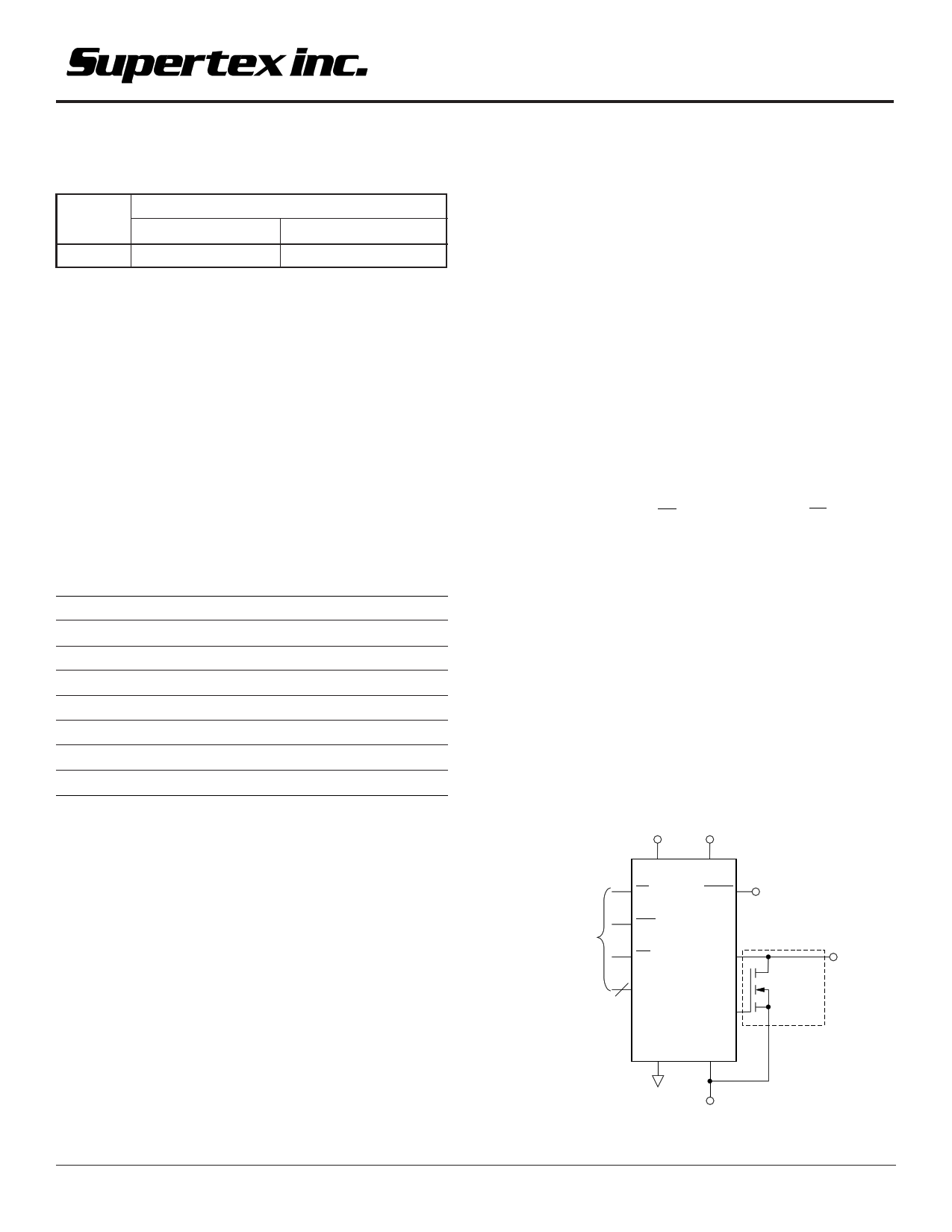
Push-Pull Configuration
* VN2222NC is an N-channel DMOS FET quad array recommended for use in
conjunction with HV39 outputs to form four 220V push-pull outputs. Each of the
four devices has a max RDS(ON) of 1.25Ω, min ID(ON) of 5.0 amps, and BVDSS
of 220V.
VCC
CS
VHIGH
FAULT
5V
Digital
Control
ENA
HV39
OE PD0
•
4
D0 – D3
•
PD3
GND
DRV0
•
•
DRV3
VLL
220V
Push-Pull
Output
*VN2222NC
(1 of 4
FETs)
VLL
12/13/01
Supertex Inc. does not recommend the use of its products in life support applications and will not knowingly sell its products for use in such applications unless it receives an adequate "products liability
indemnification insurance agreement." Supertex does not assume responsibility for use of devices described and limits its liability to the replacement of devices determined to be defective due to
workmanship. No responsibility is assumed for possible omissions or inaccuracies. Circuitry and s1pecifications are subject to change without notice. For the latest product specifications, refer to the
Supertex website: http://www.supertex.com. For complete liability information on all Supertex products, refer to the most current databook or to the Legal/Disclaimer page on the Supertex website.
1 page 
Pin Configurations
20 Pin, 300 Mil Wide Package
Pin Function
1 D1
2 D2
3 D3
4 VLL
5 GND
6 DRV3
7 DRV2
8 PD3
9 PD2
10 PD1
Pin Function
11 PD0
12 DRV1
13 DRV0
14 VPP
15 VCC
16 ENA
17 OE
18 CS
19 Fault
20 D0
28 Pin, J-Lead Package
Pin Function
1 D1
2 D2
3 D3
4 N/C
5 VLL
6 GND
7 N/C
8 DRV3
9 DRV2
10 N/C
11 PD3
12 N/C
13 PD2
14 N/C
Pin Function
15 PD1
16 PD0
17 N/C
18 DRV1
19 DRV0
20 N/C
21 VPP
22 N/C
23 VCC
24 ENA
25 OE
26 CS
27 Fault
28 D0
Package Outline
1 20
2 19
3 18
4 17
5 16
6 15
7 14
8 13
9 12
10 11
20 Pin, 300 Mil Wide DIP
HV3922C
HV3922
25 24 23 22 21 20 19
26 18
27 17
28 16
1 15
2 14
3 13
4 12
5 6 7 8 9 10 11
28 Pin J-Lead Package
HV3922DJ
20 Pin, 300 Mil Wide Package
Pin Function
1S
2S
3S
4 G1
5 G2
6 G3
7 G4
8S
9S
10 S
Pin Function
11 S
12 S
13 N/C
14 D4
15 D3
16 D2
17 D1
18 N/C
19 S
20 S
©2001 Supertex Inc. All rights reserved. Unauthorized use or reproduction prohibited.
5
1 20
2 19
3 18
4 17
5 16
6 15
7 14
8 13
9 12
10 11
20 Pin, 300 Mil Wide DIP
VN2222NC
12/13/010
1235 Bordeaux Drive, Sunnyvale, CA 94089
TEL: (408) 744-0100 • FAX: (408) 222-4895
www.supertex.com
5 Page | ||
| Páginas | Total 5 Páginas | |
| PDF Descargar | [ Datasheet HV3922DJ.PDF ] | |
Hoja de datos destacado
| Número de pieza | Descripción | Fabricantes |
| HV3922DJ | High Voltage PIN Diode Driver | Supertex Inc |
| Número de pieza | Descripción | Fabricantes |
| SLA6805M | High Voltage 3 phase Motor Driver IC. |
Sanken |
| SDC1742 | 12- and 14-Bit Hybrid Synchro / Resolver-to-Digital Converters. |
Analog Devices |
|
DataSheet.es es una pagina web que funciona como un repositorio de manuales o hoja de datos de muchos de los productos más populares, |
| DataSheet.es | 2020 | Privacy Policy | Contacto | Buscar |