|
|
|
PDF AD1891 Data sheet ( Hoja de datos )
| Número de pieza | AD1891 | |
| Descripción | SamplePort Stereo Asynchronous Sample Rate Converters | |
| Fabricantes | Analog Devices | |
| Logotipo | ||
Hay una vista previa y un enlace de descarga de AD1891 (archivo pdf) en la parte inferior de esta página. Total 20 Páginas | ||
|
No Preview Available !
a
SamplePort Stereo Asynchronous
Sample Rate Converters
AD1890/AD1891
FEATURES
Automatically Sense Sample Frequencies—No
Programming Required
Tolerant of Sample Clock Jitter
Smooth Transition When Sample Clock Frequencies
Cross
Accommodate Dynamically Changing Asynchronous
Sample Clocks
8 kHz to 56 kHz Sample Clock Frequency Range
1:2 to 2:1 Ratio Between Sample Clocks
–106 dB THD+N at 1 kHz (AD1890)
120 dB Dynamic Range (AD1890)
Optimal Clock Tracking Control
–Short/Long Group Delay Modes
–Slow/Fast Settling Modes
Linear Phase in All Modes
Equivalent of 4 Million 22-Bit FIR Filter Coefficients
Stored On-Chip
Automatic Output Mute
Flexible Four Wire Serial Interfaces
Low Power
APPLICATIONS
Digital Mixing Consoles and Digital Audio Workstations
CD-R, DAT, DCC and MD Recorders
Multitrack Digital Audio and Video Tape Recorders
Studio to Transmitter Links
Digital Audio Signal Routers/Switches
Digital Audio Broadcast Equipment
High Quality D/A Converters
Digital Tape Recorder Varispeed Applications
Computer Communication and Multimedia Systems
PRODUCT OVERVIEW
The AD1890 and AD1891 SamplePorts™ are fully digital, stereo
Asynchronous Sample Rate Converters (ASRCs) that solve sample
rate interfacing and compatibility problems in digital audio equip-
ment. Conceptually, these converters interpolate the input data up
to a very high internal sample rate with a time resolution of 300 ps,
then decimate down to the desired output sample rate. The
AD1890 is intended for 18- and 20-bit professional applications,
and the AD1891 is intended for 16-bit lower cost applications
where large dynamic sample-rate changes are not encountered.
These devices are asynchronous because the frequency and phase
relationships between the input and output sample clocks (both are
inputs to the AD1890/AD1891 ASRCs) are arbitrary and need not
be related by a simple integer ratio. There is no need to explicitly
select or program the input and output sample clock frequencies, as
the AD1890/AD1891 automatically sense the relationship between
SamplePort and SamplePorts are trademarks of Analog Devices, Inc.
REV. 0
Information furnished by Analog Devices is believed to be accurate and
reliable. However, no responsibility is assumed by Analog Devices for its
use, nor for any infringements of patents or other rights of third parties
which may result from its use. No license is granted by implication or
otherwise under any patent or patent rights of Analog Devices.
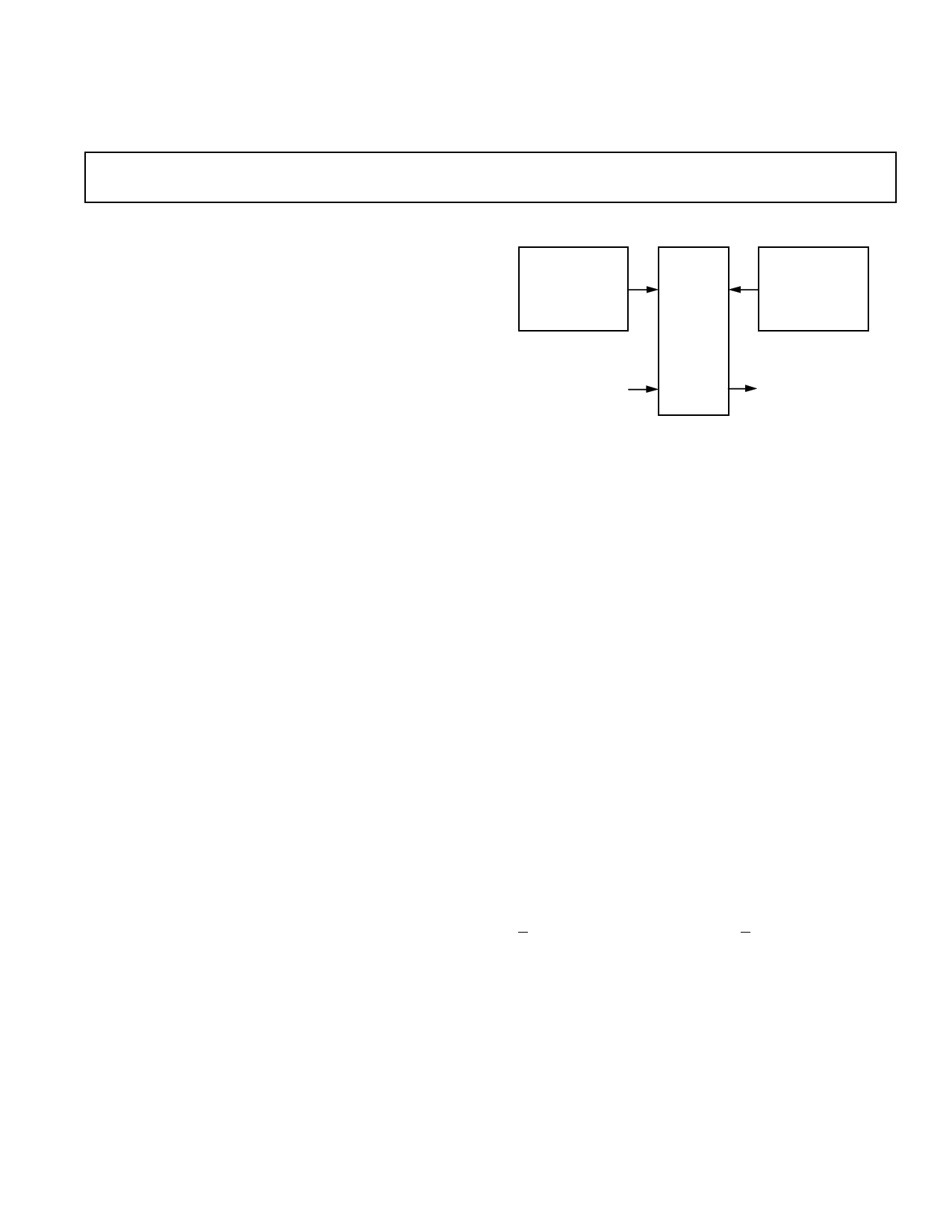
SYSTEM DIAGRAM
EXAMPLE
FREQUENCIES:
DAT 48kHz OR
CD 44.1kHz OR
BROADCAST 32kHz
INPUT SAMPLE CLOCK
AD1890/
AD1891
EXAMPLE
FREQUENCIES:
DAT 48kHz OR
CD 44.1kHz OR
BROADCAST 32kHz
OUTPUT SAMPLE CLOCK
INPUT SERIAL DATA
OUTPUT SERIAL DATA
the two clocks. The input and output sample clock frequencies
can nominally range from 8 kHz to 56 kHz, and the ratio
between them can vary from 1:2 to 2:1.
The AD1890/AD1891 use multirate digital signal processing
techniques to construct an output sample stream from the input
sample stream. The input word width is 4 to 20 bits for the
AD1890 or 4 to 16 bits for the AD1891. Shorter input words
are automatically zero-filled in the LSBs. The output word
width for both devices is 24 bits. The user can receive as many
of the output bits as desired. Internal arithmetic is performed
with 22-bit coefficients and 27-bit accumulation. The digital
samples are processed with unity gain.
The input and output control signals allow for considerable flex-
ibility for interfacing to a variety of DSP chips, AES/EBU
receivers and transmitters and for I2S compatible devices. Input
and output data can be independently justified to the left/right
clock edge, or delayed by one bit clock from the left/right clock
edge. Input and output data can also be independently justified
to the word clock rising edge or delayed by one bit clock from
the word clock rising edge. The bit clocks can also be indepen-
dently configured for rising edge active or falling edge active
operation.
The AD1890/AD1891 SamplePort™ ASRCs have on-chip digi-
tal coefficients that correspond to a highly oversampled 0 kHz to
20 kHz low-pass filter with a flat passband, a very narrow tran-
sition band, and a high degree of stopband attenuation. A subset
of these filter coefficients are dynamically chosen on the basis of
the filtered instantaneous ratio between the input sample clock
(LR_I) and the output sample clock (LR_O), and these coeffi-
cients are used in an FIR convolver to perform the sample rate
conversion. Refer to the “Theory of Operation” section of this
data sheet for a more thorough functional description. The low-
pass filter has been designed so that full 20 kHz bandwidth is
maintained when the input and output sample clock frequencies
are as low as 44.1 kHz. If the output sample rate drops below
the input sample rate, the bandwidth of the input signal is
(continued on Page 4)
One Technology Way, P.O. Box 9106, Norwood, MA 02062-9106, U.S.A.
Tel: 617/329-4700
Fax: 617/326-8703
1 page 
AD1890/AD1891
DEFINITIONS
Dynamic Range
The ratio of a near full-scale input signal to the integrated noise
in the passband (0 to ≈20 kHz), expressed in decibels (dB). Dy-
namic range is measured with a –60 dB input signal and
“60 dB” arithmetically added to the result.
Total Harmonic Distortion + Noise
Total Harmonic Distortion plus Noise (THD+N) is defined as
the ratio of the square root of the sum of the squares of the val-
ues of the harmonics and noise to the rms value of a sinusoidal
input signal. It is usually expressed in percent (%) or decibels.
Interchannel Phase Deviation
Difference in input sampling times between stereo channels, ex-
pressed as a phase difference in degrees between 1 kHz inputs.
Group Delay
Intuitively, the time interval required for a full-level input pulse
to appear at the converter’s output, at full level, expressed in
milliseconds (ms). More precisely, the derivative of radian phase
with respect to radian frequency at a given frequency.
Transport Delay
The time interval between when an impulse is applied to the
converters input and when the output starts to be affected by
this impulse, expressed in milliseconds (ms). Transport delay is
independent of frequency.
AD1890/AD1891 PIN LIST
Serial Input Interface
Pin Name Number I/O Description
DATA_I 3
BCLK_I 4
WCLK_I 5
LR_I
6
I Serial input, MSB first, containing two channels of 4- to 20-bits of twos-complement data per
channel. AD1891 ONLY: Maximum of 16 data bits per channel; additional bits ignored.
I Bit clock input for input data.
I Word clock input for input data. This input is rising edge sensitive. (Not required in LR input data
clock triggered mode [TRGLR_I = HI].)
I Left/right clock input for input data. Must run continuously.
Serial Output Interface
Pin Name Number I/O Description
DATA_O 23
BCLK_O 26
WCLK_O 25
LR_O
24
O Serial output, MSB first, containing two channels of 4- to 24-bits of twos-complement data per
channel.
I Bit clock input for output data.
I Word clock input for output data. This input is rising edge sensitive. (Not required in LR output
data clock triggered mode [TRGLR_O = HI].)
I Left/right clock input for output data. Must run continuously.
Input Control Signals
Pin Name Number I/O Description
BKPOL_I 10
TRGLR_I 11
MSBDLY_I 12
I Bit clock polarity. LO: Normal mode. Input data is sampled on rising edges of BCLK_I. HI:
Inverted mode. Input data is sampled on falling edges of BCLK_I.
I Trigger on LR_I. HI: Changes in LR_I indicate beginning1 of valid input data. LO: Rising edge of
WCLK_I indicates beginning of valid input data.
I MSB delay. HI: Input data is delayed one BCLK_I after either LR_I (TRGLR_I = HI) or WCLK_I
(TRGLR_I = LO) indicates the beginning of valid input data. Included for I2S data format
compatibility. LO: No delay.
NOTE
1The beginning of valid data will be delayed by one BLCK_I if MSBDEL_I is selected (HI).
REV. 0
–5–
5 Page 
AD1890/AD1891
Sample Clock Jitter Rejection
The loop filter settling time also affects the ability of the
AD1890/AD1891 ASRCs to reject sample clock jitter, since the
control loop effectively computes a time weighted average or
“estimated” new output of many past input and output clock
events. This first order low pass filtering of the sample clock
ratio provide the AD1890/AD1891 with their jitter rejection
characteristic. In the slow settling mode, the AD1890/AD1891
attenuate jitter frequencies higher than 3 Hz (≈800 ms for the
control loop to settle to an 18-bit “pure” sine wave), and thus
reject all but the most severe sample clock jitter; performance is
essentially limited only by the FIR filter. In the fast settling
mode, the ASRCs attenuate jitter components above 12 Hz
(≈200 ms for the control loop to settle). Due to the effects of
on-chip synchronization of the sample clocks to the 16 MHz
(62.5 ns) MCLK master clock, sample clock jitter must be a
large percentage of the MCLK period (>10 ns) before perfor-
mance degrades in either the slow or fast settling modes. Note
that since both past input and past output clocks are used to
compute the filtered “current” internal output clock request, jit-
ter on both the input sample clock and the output sample clock
is rejected equally. In summary: the fast settling mode is best for
applications when the sample rates will be dynamically altered
(e.g., varispeed situations) while the slow settling mode provides
the most sample clock jitter rejection.
Clock jitter can be modeled as a frequency modulation process.
Figure 7 shows one such model, where a noise source combined
with a sine wave source modulates the “carrier” frequency gen-
erated by a voltage controlled oscillator.
NOISE SOURCE
NOISE
WAVEFORM
SINE
WAVE
VOLTAGE
SOURCE
Σ VCO
ANALOG IN
ADC
DIGITAL
OUT
Figure 7. Clock Jitter Modeled as a Modulated VCO
If the jittered output of the VCO is used to clock an analog-to-
digital converter, the digital output of the ADC will be contami-
nated by the presence of jitter. If the noise source is spectrally
flat (i.e., “white” jitter), then an FFT of the ADC digital output
would show a spectrum with a uniform noise floor which is el-
evated compared to the spectrum with the noise source turned
off. If the noise source has distinct frequency components (i.e.,
“correlated” jitter), then an FFT of the ADC digital output
would show symmetrical sidebands around the ADC input sig-
nal, at amplitudes and frequencies determined by frequency
modulation theory. One notable result is that the level of the
noise or the sidebands is proportional to the slope of the input
signal, i.e., the worst case occurs at the highest frequency full-
scale input (a full-scale 20 kHz sinusoid).
The AD1890/AD1891 apply rejection to these jitter frequency
components referenced to the input signal. In other words, if a
5 kHz digital sinusoid is applied to the ASRC, depending on the
settling mode selected, the ASRC will attenuate sample clock
jitter at either 3 Hz above and below 5 kHz (slow settling) or
12 Hz above and below 5 kHz (fast settling). The rolloff is 6 dB
per octave. As an example, suppose there was correlated jitter
present on the input sample clock with a 1 kHz component,
associated with the same 5 kHz sinusoidal input data. This
would produce sidebands at 4 kHz and 6 kHz, 3 kHz and
7 kHz, etc., with amplitudes that decrease as they move away
from the input signal frequency. For the slow settling mode
case, 1 kHz represents more than nine octaves (relative to
3 Hz), so the first two sideband pairs would be attenuated by
more than 54 dB. For the fast settling mode case, 1 kHz repre-
sents more than seven octaves (relative to 12 Hz), so that the
first two sideband pairs would be attenuated by more than
42 dB. The second and higher sideband pairs are attenuated
even more because they are spaced further from the input signal
frequency.
Group Delay Modes
The other parameter that determines the likelihood of FIFO in-
put overflow or output underflow is the FIFO depth. This is the
parameter that is selected by the GPDLYS pin (AD1890 only;
this pin is a No Connect for the AD1891). The drawback with
increasing the FIFO depth is increasing the device’s overall
group delay, but most applications are insensitive to a small in-
crease in group delay. [This FIFO-induced group delay is better
termed transport delay, since it is frequency independent, and
should be kept conceptually distinct from the notion of group
delay as used in the polyphase filter bank model. The total
group delay of the AD1890/AD1891 equals the FIFO transport
delay plus the FIR (polyphase) filter group delay.]
In the short group delay mode, the FIFO read and write point-
ers are separated by five memory locations (≈100 µs equivalent
transport delay at a 50 kHz sample rate). This is added to the
FIR filter delay (64 taps divided by 2) for a total nominal group
delay in short mode of ≈700 µs. The short group delay mode is
useful when the input and output sample clocks are asynchro-
nous but either do not vary or change very slowly.
In the long group delay mode (AD1890 only, the AD1891 is
always in the short group delay mode), the FIFO read and write
pointers are separated by 96 memory locations (≈2 ms equiva-
lent transport delay). This is added to the FIR filter delay
(64 taps divided by 2) for a total nominal group delay in long
mode of ≈3 ms. The long group delay mode is useful when the
input and output sample clocks are asynchronous and changing
relative to one another, such as during varispeed effects.
These delays are deterministic and constant except when FSOUT
drops below FSIN which causes the number of FIR filter taps to
increase (see “Cutoff Frequency Modification” below). In either
mode, if the FIFO read and write addresses cross, the MUTE_O
signal will be asserted. Note that in all modes and under all con-
ditions, both the highly oversampled low-pass prototype and the
polyphase subfilters of the AD1890/AD1891 ASRCs possess a
linear phase response.
The AD1890 has been designed so that when it is in long group
delay mode and fast settling mode, a full 2:1 step change (i.e.,
occurring between two samples) in sample frequency ratio can
be tolerated without output mute.
REV. 0
–11–
11 Page | ||
| Páginas | Total 20 Páginas | |
| PDF Descargar | [ Datasheet AD1891.PDF ] | |
Hoja de datos destacado
| Número de pieza | Descripción | Fabricantes |
| AD1890 | SamplePort Stereo Asynchronous Sample Rate Converters | Analog Devices |
| AD1891 | SamplePort Stereo Asynchronous Sample Rate Converters | Analog Devices |
| AD1892 | Integrated Digital Receiver/Rate Converter | Analog Devices |
| AD1893 | Low Cost SamplePort 16-Bit Stereo Asynchronous Sample Rate Converter | Analog Devices |
| Número de pieza | Descripción | Fabricantes |
| SLA6805M | High Voltage 3 phase Motor Driver IC. |
Sanken |
| SDC1742 | 12- and 14-Bit Hybrid Synchro / Resolver-to-Digital Converters. |
Analog Devices |
|
DataSheet.es es una pagina web que funciona como un repositorio de manuales o hoja de datos de muchos de los productos más populares, |
| DataSheet.es | 2020 | Privacy Policy | Contacto | Buscar |