|
|
|
PDF AD1854 Data sheet ( Hoja de datos )
| Número de pieza | AD1854 | |
| Descripción | Stereo/ 96 kHz/ Multibit DAC | |
| Fabricantes | Analog Devices | |
| Logotipo | ||
Hay una vista previa y un enlace de descarga de AD1854 (archivo pdf) en la parte inferior de esta página. Total 12 Páginas | ||
|
No Preview Available !
a
Stereo, 96 kHz, Multibit ⌺⌬ DAC
AD1854
FEATURES
5 V Stereo Audio DAC System
Accepts 16-/18-/20-/24-Bit Data
Supports 24 Bits and 96 kHz Sample Rate
Multibit Sigma-Delta Modulator with “Perfect Differential
Linearity Restoration” for Reduced Idle Tones and
Noise Floor
Data Directed Scrambling DAC—Least Sensitive to Jitter
Differential Output for Optimum Performance
113 dB Dynamic Range at 48 kHz Sample Rate
(AD1854KRS)
112 dB Signal-to-Noise at 48 kHz Sample Rate
(AD1854KRS)
–101 THD+N (AD1854KRS)
On-Chip Volume Control with 1024 Steps
Hardware and Software Controllable Clickless Mute
Zero Input Flag Outputs for Left and Right Channels
Digital De-Emphasis Processing
Supports 256 ؋ FS or 384 ؋ FS Master Mode Clock
Switchable Clock Doubler
Power-Down Mode Plus Soft Power-Down Mode
Flexible Serial Data Port with Right-Justified, Left-
Justified, and I2S-Compatible
28-Lead SSOP Plastic Package
APPLICATIONS
DVD, CD, Set-Top Boxes, Home Theater Systems,
Automotive Audio Systems, Sampling Musical
Keyboards, Digital Mixing Consoles, Digital Audio
Effects Processors
PRODUCT OVERVIEW
The AD1854 is a high performance, single-chip stereo, audio
DAC delivering 113 dB Dynamic Range and 112 dB SNR
(A-weighted—not muted) at 48 kHz sample rate. It is comprised
of a multibit sigma-delta modulator with dither, continuous
time analog filters and analog output drive circuitry. Other features
include an on-chip stereo attenuator and mute, programmed
through an SPI-compatible serial control port. The AD1854
is fully compatible with current DVD formats, including 96 kHz
sample frequency and 24 bits. It is also backwards compatible
by supporting 50 µs/15 µs digital de-emphasis intended for
“redbook” 44.1 kHz sample frequency playback from com-
pact discs.
The AD1854 has a very simple but very flexible serial data input
port that allows for glueless interconnection to a variety of ADCs,
DSP chips, AES/EBU receivers and sample rate converters.
The AD1854 can be configured in left-justified, I2S, and right-
justified. The AD1854 accepts serial audio data in MSB first,
twos-complement format. A power-down mode is offered to mini-
mize power consumption when the device is inactive. The AD1854
operates from a single 5 V power supply. It is fabricated on a single
monolithic integrated circuit and housed in a 28-lead SSOP
package for operation over the temperature range 0°C to 70°C.
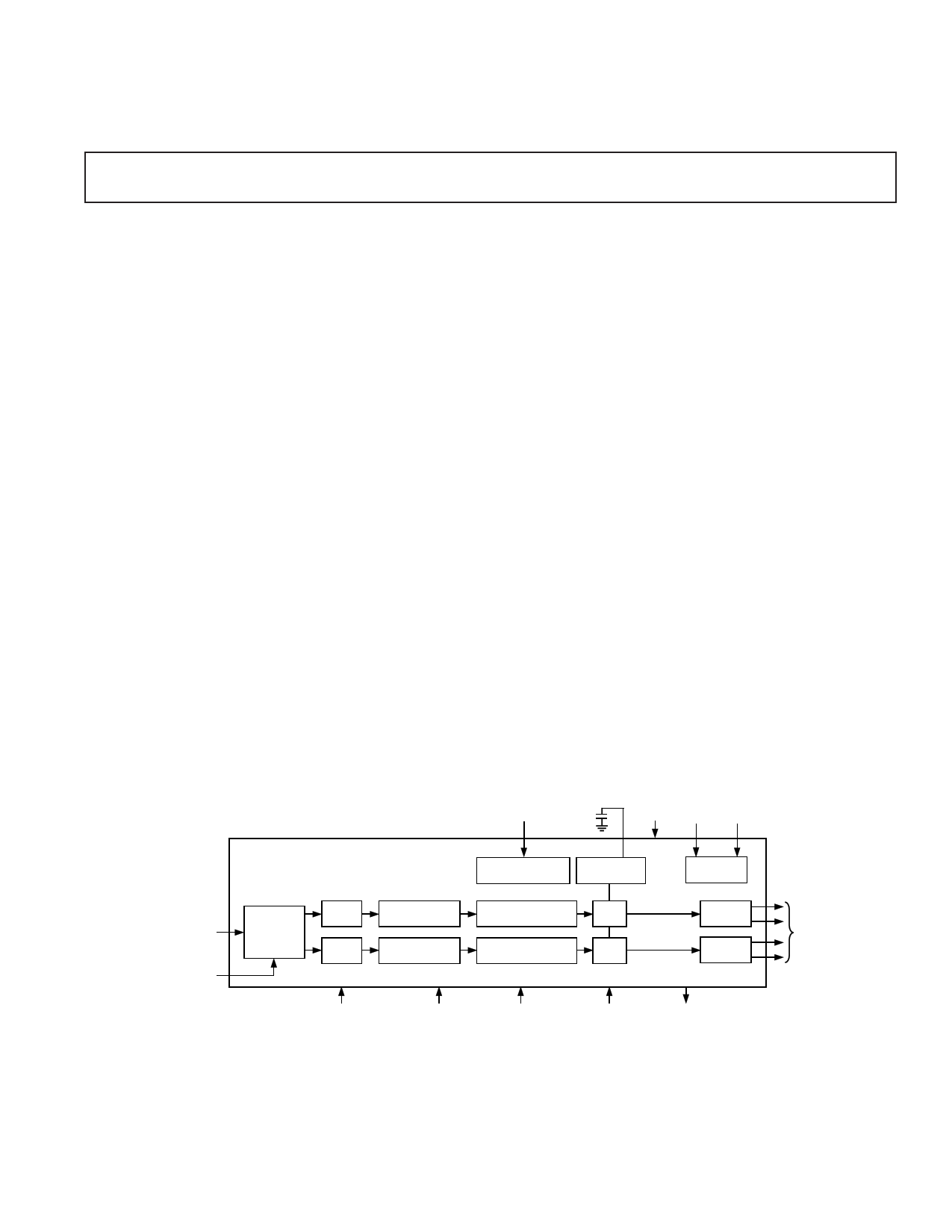
FUNCTIONAL BLOCK DIAGRAM
CONTROL DATA
VOLUME INPUT
MUTE
3
DIGITAL CLOCK 96/48FS
SUPPLY IN CLOCK
2
AD1854
SERIAL CONTROL VOLTAGE
INTERFACE
REFERENCE
16-/18-/20-/24-BIT
DIGITAL
DATA INPUT
SERIAL 2
MODE
SERIAL
DATA
INTERFACE
ATTEN/
MUTE
ATTEN/
MUTE
PD /RST
8 ؋ FS
INTERPOLATOR
8 ؋ FS
INTERPOLATOR
MUTE
MULTIBIT SIGMA-
DELTA MODULATOR
MULTIBIT SIGMA-
DELTA MODULATOR
DAC
DAC
DE-EMPHASIS
2
ANALOG
SUPPLY
CLOCK
CIRCUIT
OUTPUT
BUFFER
OUTPUT
BUFFER
2
ZERO
FLAG
ANALOG
OUTPUTS
REV. A
Information furnished by Analog Devices is believed to be accurate and
reliable. However, no responsibility is assumed by Analog Devices for its
use, nor for any infringements of patents or other rights of third parties
which may result from its use. No license is granted by implication or
otherwise under any patent or patent rights of Analog Devices.
One Technology Way, P.O. Box 9106, Norwood, MA 02062-9106, U.S.A.
Tel: 781/329-4700 World Wide Web Site: http://www.analog.com
Fax: 781/326-8703
© Analog Devices, Inc., 2000
1 page 
Pin Input/Output
1I
2I
3I
4I
5I
6I
7I
8O
9I
10
11, 15
12
13
14
I
I
O
O
O
16 O
17 O
18 I
19 O
20 I
21 I
22 O
23 I
24 I
25 I
26 I
27 I
28 I
AD1854
Pin Name
DGND
MCLK
CLATCH
CCLK
CDATA
384/256
X2MCLK
ZEROR
DEEMP
96/48
AGND
OUTR+
OUTR–
FILTR
OUTL–
OUTL+
AVDD
FILTB
IDPM1
IDPM0
ZEROL
MUTE
PD/RST
L/RCLK
BCLK
SDATA
DVDD
PIN FUNCTION DESCRIPTIONS
Description
Digital Ground.
Master Clock Input. Connect to an external clock source at either 256, 384
or 512 FS.
Latch input for control data. This input is rising-edge sensitive.
Control clock input for control data. Control input data must be valid on the
rising edge of CCLK. CCLK may be continuous or gated.
Serial control input, MSB first, containing 16 bits of unsigned data per
channel. Used for specifying channel-specific attenuation and mute.
Selects the master clock mode as either 384 times the intended sample
frequency (HI) or 256 times the intended sample frequency (LO). The state
of this input should be hardwired to logic HI or logic LO, or may be changed
while the AD1854 is in power-down/reset. It must not be changed while the
AD1854 is operational.
Selects internal clock doubler (LO) or internal clock = MCLK (HI).
Right Channel Zero Flag Output. This pin goes HI when Right Channel has
no signal input for more than 1024 LR Clock Cycles.
De-Emphasis. Digital de-emphasis is enabled when this input signal is HI.
This is used to impose a 50 µs/15 µs response characteristic on the output
audio spectrum at an assumed 44.1 kHz sample rate.
Selects 48 kHz (LO) or 96 kHz Sample Frequency Control.
Analog Ground.
Right Channel Positive line level analog output.
Right Channel Negative line level analog output.
Voltage Reference Filter Capacitor Connection. Bypass and decouple the
voltage reference with parallel 10 µF and 0.1 µF capacitors to the AGND.
Left Channel Negative line level analog output.
Left Channel Positive line level analog output.
Analog Power Supply. Connect to analog 5 V supply.
Filter Capacitor connection, connect 10 µF capacitor to AGND.
Input serial data port mode control one. With IDPM0, defines one of four
serial modes.
Input serial data port mode control zero. With IDPM1, defines one of four
serial modes.
Left Channel Zero Flag Output. This pin goes HI when Left Channel has no
signal input for more than 1024 LR Clock Cycles.
Mute. Assert HI to mute both stereo analog outputs. Deassert LO for nor-
mal operation.
Power-Down/Reset. The AD1854 is placed in a low power consumption
mode when this pin is held LO. The AD1854 is reset on the rising edge of
this signal. The serial control port registers are reset to the default values.
Connect HI for normal operation.
Left/Right clock input for input data. Must run continuously.
Bit clock input for input data. Need not run continuously; may be gated or
used in a burst fashion.
Serial input, MSB first, containing two channels of 16, 18, 20, and 24 bits of
twos complement data per channel.
Digital Power Supply Connect to digital 5 V supply.
REV. A
–5–
5 Page 
AD1854
TYPICAL PERFORMANCE
Figures 13 through 20 illustrate the typical analog performance
of the AD1854 as measured by an Audio Precision System Two.
Signal-to-Noise and THD+N performance are shown under a
range of conditions. Figure 14 shows the power supply rejection
performance of the AD1854. Figure 15 shows the noise floor of
the AD1854. The digital filter transfer function is shown in
Figure 16. The two-tone test in Figure 17 is per the SMPTE
Standard for Measuring Intermodulation Distortion.
–60
–65
–70
–75
–80
–85
–90
–95
–100
–105
–110
–115
–120
–125
–130
–135
–60
–65
–70
–75
–80
–85
–90
–95
–100
–105
–110
–115
–120
–125
–130
–135
–140
–140
–145
–145
–150
–150
–155
–155
–160
–160
0 2 4 6 8 10 12 14 16 18 20
FREQUENCY – kHz
Figure 13. THD+N at 1 kHz, –0.5 dBFS (8K-Point FFT)
00
–20 –20
–40 –40
–60 –60
–80 –80
–100
–100
–120
–120 –110 –100 –90 –80 –70 –60 –50 –40 –30 –20 –10
AMPLITUDE – dBFS
–120
0
Figure 16. THD+N vs. Level at 1 kHz
–40 –40
–45 –45
–50 –50
–55 –55
–60 –60
–65 –65
–70 –70
–75 –75
–80 –80
–85 –85
–90 –90
–95
–100
–95
–100
–105
–105
–110
–110
0 2 4 6 8 10 12 14 16 18 20
FREQUENCY – kHz
Figure 14. THD+N vs. Frequency at –0.5 dBFS
–40 –40
–45 –45
–50 –50
–55 –55
–60 –60
–65 –65
–70 –70
–75 –75
–80 –80
–85 –85
–90
20 50
100 200 500 1k 2k
FREQUENCY – Hz
–90
5k 10k 20k
Figure 17. Power Supply Rejection to 300 mV p-p on AVDD
00
–10 –10
–20 –20
–30 –30
–40 –40
–50 –50
–60 –60
–70 –70
–80 –80
–90 –90
–100
–110
–120
–130
–100
–110
–120
–130
–140
–140
–150
–150
–160
–160
0 2 4 6 8 10 12 14 16 18 20
FREQUENCY – kHz
Figure 15. Dynamic Range: 1 kHz at –60 dBFS
(8K Point FFT)
REV. A
0
–10
–20
–30
–40
–50
–60
–70
–80
–90
–100
–110
–120
–130
–140
–150
–160
02 4
0
–10
–20
–30
–40
–50
–60
–70
–80
–90
–100
–110
–120
–130
–140
–150
–160
6 8 10 12 14 16 18 20
FREQUENCY – kHz
Figure 18. Noise Floor, A-Weighted (8K-Point FFT)
–11–
11 Page | ||
| Páginas | Total 12 Páginas | |
| PDF Descargar | [ Datasheet AD1854.PDF ] | |
Hoja de datos destacado
| Número de pieza | Descripción | Fabricantes |
| AD1851 | 16-Bit/18-Bit/ 16 X Fs PCM Audio DACs | Analog Devices |
| AD1852 | Stereo/ 24-Bit/ 192 kHz Multibit DAC | Analog Devices |
| AD1853 | Stereo/ 24-Bit/ 192 kHz/ Multibit DAC | Analog Devices |
| AD1854 | Stereo/ 96 kHz/ Multibit DAC | Analog Devices |
| Número de pieza | Descripción | Fabricantes |
| SLA6805M | High Voltage 3 phase Motor Driver IC. |
Sanken |
| SDC1742 | 12- and 14-Bit Hybrid Synchro / Resolver-to-Digital Converters. |
Analog Devices |
|
DataSheet.es es una pagina web que funciona como un repositorio de manuales o hoja de datos de muchos de los productos más populares, |
| DataSheet.es | 2020 | Privacy Policy | Contacto | Buscar |