|
|
|
PDF AD5533 Data sheet ( Hoja de datos )
| Número de pieza | AD5533 | |
| Descripción | 32-Channel Infinite Sample-and-Hold | |
| Fabricantes | Analog Devices | |
| Logotipo | ||
Hay una vista previa y un enlace de descarga de AD5533 (archivo pdf) en la parte inferior de esta página. Total 16 Páginas | ||
|
No Preview Available !
a
32-Channel Infinite
Sample-and-Hold
AD5533*
FEATURES
Infinite Sample-and-Hold Capability to ؎0.018% Accuracy
High Integration: 32-Channel SHA in 12 ؋ 12 mm2 LFBGA
Per Channel Acquisition Time of 16 s max
Adjustable Voltage Output Range
Output Voltage Span 10 V
Output Impedance 0.5 ⍀
Readback Capability
DSP-/Microcontroller-Compatible Serial Interface
Parallel Interface
Temperature Range –40؇C to +85؇C
APPLICATIONS
Level Setting
Instrumentation
Automatic Test Equipment
Industrial Control Systems
Data Acquisition
Low Cost I/O
GENERAL DESCRIPTION
The AD5533 combines a 32-channel voltage translation function
with an infinite output hold capability. An analog input voltage
on the common input pin, VIN, is sampled and its digital repre-
sentation transferred to a chosen DAC register. VOUT for this
DAC is then updated to reflect the new contents of the DAC
register. Channel selection is accomplished via the parallel address
inputs A0–A4 or via the serial input port. The output voltage
range is determined by the offset voltage at the OFFS_IN pin
and the gain of the output amplifier. It is restricted to a range
from VSS + 2 V to VDD – 2 V because of the headroom of the
output amplifier.
The device is operated with AVCC = 5 V ± 5%, DVCC = 2.7 V to
5.25 V, VSS = –4.75 V to –16.5 V and VDD = 8 V to 16.5 V and
requires a stable 3 V reference on REF_IN as well as an offset
voltage on OFFS_IN.
PRODUCT HIGHLIGHTS
1. Infinite Droopless Sample-and-Hold Capability.
2. The AD5533 is available in a 74-lead LFBGA package with a
body size of 12 mm × 12 mm.
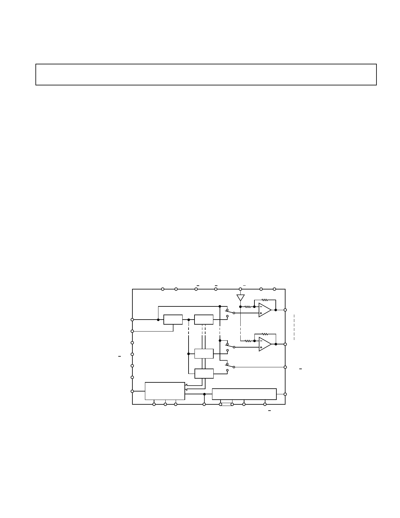
FUNCTIONAL BLOCK DIAGRAM
DVCC AVCC REF IN REF OUT OFFS IN VDD VSS
VIN
TRACK / RESET
BUSY
DAC GND
AGND
DGND
SER / PAR
ADC
DAC
VOUT 0
AD5533
INTERFACE
CONTROL
LOGIC
SCLK DIN DOUT
DAC
DAC
VOUT 31
OFFS OUT
ADDRESS INPUT REGISTER
WR
SYNC/ CS A4 –A0 CAL OFFSET SEL
*Protected by U.S. Patent No. 5,969,657; other patents pending.
REV. 0
Information furnished by Analog Devices is believed to be accurate and
reliable. However, no responsibility is assumed by Analog Devices for its
use, nor for any infringements of patents or other rights of third parties
which may result from its use. No license is granted by implication or
otherwise under any patent or patent rights of Analog Devices.
One Technology Way, P.O. Box 9106, Norwood, MA 02062-9106, U.S.A.
Tel: 781/329-4700 World Wide Web Site: http://www.analog.com
Fax: 781/326-8703
© Analog Devices, Inc., 2000
1 page 
SERIAL INTERFACE TIMING DIAGRAMS
SCLK
SYNC
DIN
t1
1234 56789
t3 t2
t4 t5
t6
MSB
Figure 3. 10-Bit Write (SHA Mode and Both Readback Modes)
AD5533
10
LSB
SCLK 10
SYNC
DOUT
t10
t1
1 2 3 4 5 6 7 8 9 10 11 12 13 14
t7 t2
t4
t8
t9
MSB
Figure 4. 14-Bit Read (Both Readback Modes)
LSB
REV. 0
–5–
5 Page 
AD5533
FUNCTIONAL DESCRIPTION
The AD5533 can be thought of as consisting of an ADC and 32
DACs in a single package. The input voltage VIN is sampled
and converted into a digital word. The digital result is loaded
into one of the DAC registers and is converted (with gain and
offset) into an analog output voltage (VOUT0–VOUT31). Since
the channel output voltage is effectively the output of a DAC
there is no droop associated with it. As long as power to the
device is maintained, the output voltage will remain constant
until this channel is addressed again.
To update a single channel’s output voltage, the required new
voltage level is set up on the common input pin, VIN. The desired
channel is then addressed via the parallel port or the serial port.
When the channel address has been loaded, provided TRACK is
high, the circuit begins to acquire the correct code to load to the
DAC in order that the DAC output matches the voltage on VIN.
The BUSY pin goes low and remains so until the acquisition is
complete. The noninverting input to the output buffer is tied to
VIN during the acquisition period to avoid spurious outputs while
the DAC acquires the correct code. The acquisition is completed
in 16 µs max. The BUSY pin goes high and the updated DAC
output assumes control of the output voltage. The output voltage
of the DAC is connected to the noninverting input of the output
buffer. The held voltage will remain on the output pin indefinitely,
without drooping, as long as power to the device is maintained.
On power-on, all the DACs, including the offset channel, are
loaded with zeros. The outputs of the DACs are at 50 mV typical
(negative full-scale). If the OFFS_IN pin is driven by the on-board
offset channel, the outputs VOUT0 to VOUT31 are also at 50 mV on
power-on since OFFS_IN = 50 mV (VOUT = 3.52 × VDAC – 3.52
× VOFFS_IN = 176 mV – 126 mV = 50 mV).
Analog Input
The equivalent analog input circuit is shown in Figure 11. The
Capacitor C1 is typically 20 pF and can be attributed to pin
capacitance and 32 off-channels. When a channel is selected, an
extra 7.5 pF (typ) is switched in. This Capacitor C2 is charged to
the previously acquired voltage on that particular channel so
it must charge/discharge to the new level. It is essential that the
external source can charge/discharge this additional capaci-
tance within 1 µs–2 µs of channel selection so that VIN can be
acquired accurately. For this reason a low impedance source is
recommended.
VIN
C1
20pF
ADDRESSED CHANNEL
C2
7.5pF
Figure 11. Analog Input Circuit
Large source impedances will significantly affect the performance
of the ADC. This may necessitate the use of an input buffer
amplifier.
Output Buffer Stage—Gain and Offset
The function of the output buffer stage is to translate the 0 V–3 V
output of the DAC to a wider range. This is done by gaining up
the DAC output by 3.52 and offsetting the voltage by the volt-
age on OFFS_IN pin.
VOUT = 3.52 × VDAC – 2.52 × VOFFS_IN
VDAC is the output of the DAC.
VOFFS_IN is the voltage at the OFFS_IN pin.
Table I shows how the output range on VOUT relates to the offset
voltage supplied by the user.
Table I. Sample Output Voltage Ranges
VOFFS_IN (V)
0.5
1
VDAC (V)
0 to 3
0 to 3
VOUT (V)
–1.26 to +9.3
–2.52 to +8.04
VOUT is limited only by the headroom of the output amplifiers.
VOUT must be within maximum ratings.
Offset Voltage Channel
The offset voltage can be externally supplied by the user at
OFFS_IN or it can be supplied by an additional offset voltage
channel on the device itself. The required offset voltage is set up
on VIN and acquired by the offset DAC. This offset channel’s
DAC output is directly connected to OFFS_OUT. By connect-
ing OFFS_OUT to OFFS_IN this offset voltage can be used as
the offset voltage for the 32-output amplifiers. It is important to
choose the offset so that VOUT is within maximum ratings.
CONTROLLER
DAC
VIN
BUSY
TRACK
ACQUISITION
CIRCUIT
OUTPUT
STAGE
AD5533
ONLY ONE CHANNEL SHOWN FOR SIMPLICITY
PIN
DRIVER
VOUT1
THRESHOLD
VOLTAGE
Figure 12. Typical ATE Circuit Using TRACK Input
DEVICE
UNDER
TEST
REV. 0
–11–
11 Page | ||
| Páginas | Total 16 Páginas | |
| PDF Descargar | [ Datasheet AD5533.PDF ] | |
Hoja de datos destacado
| Número de pieza | Descripción | Fabricantes |
| AD5530 | Serial Input/ Voltage Output 12-/14-Bit DACs | Analog Devices |
| AD5531 | Serial Input/ Voltage Output 12-/14-Bit DACs | Analog Devices |
| AD5532 | 32-Channel/ 14-Bit Voltage-Output DAC | Analog Devices |
| AD5532B | 14-Bit DAC | Analog Devices |
| Número de pieza | Descripción | Fabricantes |
| SLA6805M | High Voltage 3 phase Motor Driver IC. |
Sanken |
| SDC1742 | 12- and 14-Bit Hybrid Synchro / Resolver-to-Digital Converters. |
Analog Devices |
|
DataSheet.es es una pagina web que funciona como un repositorio de manuales o hoja de datos de muchos de los productos más populares, |
| DataSheet.es | 2020 | Privacy Policy | Contacto | Buscar |