|
|
|
PDF AD7476 Data sheet ( Hoja de datos )
| Número de pieza | AD7476 | |
| Descripción | 1 MSPS/ 12-/10-/8-Bit ADCs in 6-Lead SOT-23 | |
| Fabricantes | Analog Devices | |
| Logotipo | ||
1. AD7476 Hay una vista previa y un enlace de descarga de AD7476 (archivo pdf) en la parte inferior de esta página. Total 16 Páginas | ||
|
No Preview Available !
a
1 MSPS, 12-/10-/8-Bit ADCs
in 6-Lead SOT-23
AD7476/AD7477/AD7478
FEATURES
Fast Throughput Rate: 1 MSPS
Specified for VDD of 2.35 V to 5.25 V
Low Power:
3.6 mW Typ at 1 MSPS with 3 V Supplies
15 mW Typ at 1 MSPS with 5 V Supplies
Wide Input Bandwidth:
70 dB SNR at 100 kHz Input Frequency
Flexible Power/Serial Clock Speed Management
No Pipeline Delays
High-Speed Serial Interface
SPI™/QSPI™/MICROWIRE™/DSP Compatible
Standby Mode: 1 A Max
6-Lead SOT-23 Package
APPLICATIONS
Battery-Powered Systems
Personal Digital Assistants
Medical Instruments
Mobile Communications
Instrumentation and Control Systems
Data Acquisition Systems
High-Speed Modems
Optical Sensors
GENERAL DESCRIPTION
The AD7476/AD7477/AD7478 are, respectively, 12-bit, 10-bit,
and 8-bit, high-speed, low-power, successive-approximation
ADCs. The parts operate from a single 2.35 V to 5.25 V power
supply and feature throughput rates up to 1 MSPS. The parts
contain a low-noise, wide bandwidth track/hold amplifier that can
handle input frequencies in excess of 1 MHz.
The conversion process and data acquisition are controlled
using CS and the serial clock, allowing the devices to interface
with microprocessors or DSPs. The input signal is sampled on
the falling edge of CS and the conversion is also initiated at this
point. There are no pipelined delays associated with the part.
The AD7476/AD7477/AD7478 use advanced design techniques
to achieve very low-power dissipation at high throughput rates.
The reference for the part is taken internally from VDD. This
allows the widest dynamic input range to the ADC. Thus the
analog input range for the part is 0 to VDD. The conversion rate
is determined by the SCLK.
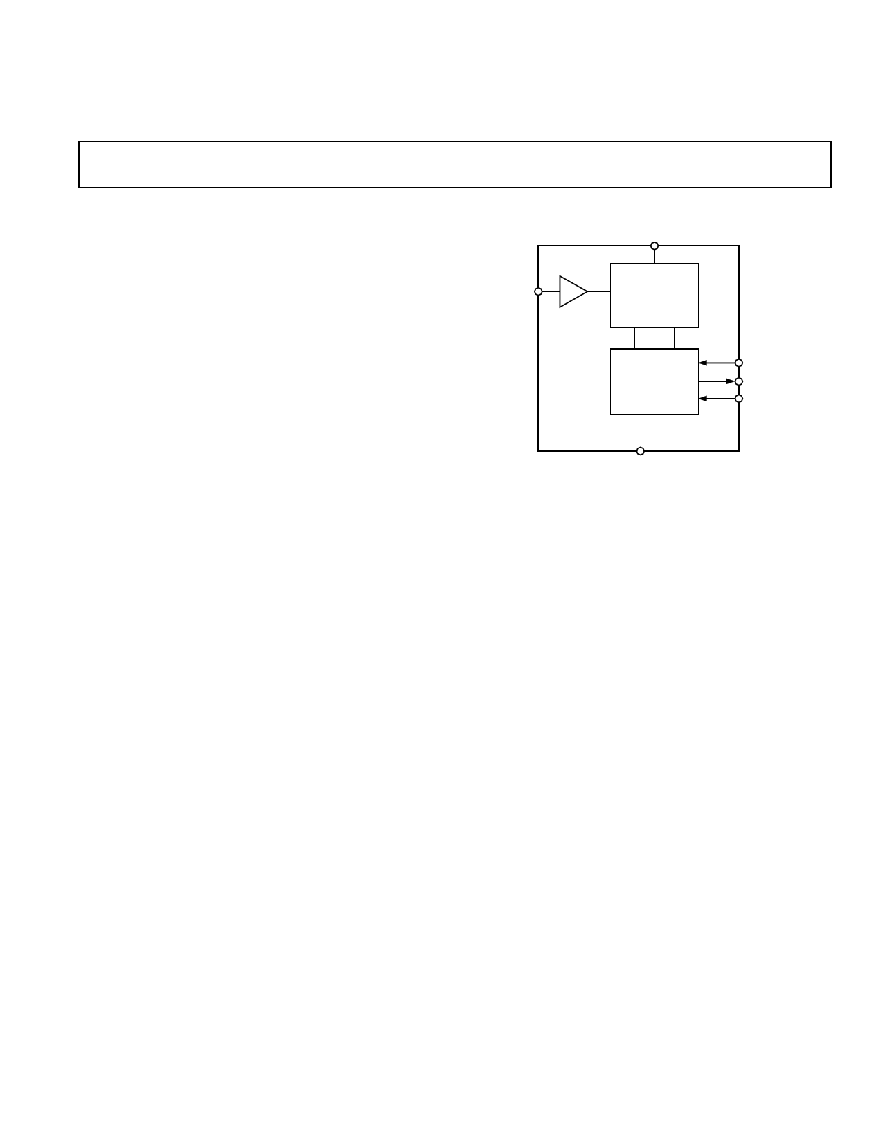
FUNCTIONAL BLOCK DIAGRAM
VDD
VIN T/H
8-/10-/12-BIT
SUCCESSIVE
APPROXIMATION
ADC
CONTROL
LOGIC
SCLK
SDATA
CS
AD7476/AD7477/AD7478
GND
PRODUCT HIGHLIGHTS
1. First 12-/10-/8-bit ADCs in an SOT-23 package.
2. High Throughput with Low Power Consumption.
3. Flexible Power/Serial Clock Speed Management.
The conversion rate is determined by the serial clock, allowing
the conversion time to be reduced through the serial clock speed
increase. This allows the average power consumption to be
reduced while not converting. The part also features a shut-
down mode to maximize power efficiency at lower throughput
rates. Power consumption is 1 µA max when in shutdown.
4. Reference derived from the power supply.
5. No Pipeline Delay.
The parts feature a standard successive-approximation ADC
with accurate control of the sampling instant via a CS input
and once-off conversion control.
SPI and QSPI are trademarks of Motorola, Inc.
MICROWIRE is a trademark of National Semiconductor Corporation.
REV. A
Information furnished by Analog Devices is believed to be accurate and
reliable. However, no responsibility is assumed by Analog Devices for its
use, nor for any infringements of patents or other rights of third parties
which may result from its use. No license is granted by implication or
otherwise under any patent or patent rights of Analog Devices.
One Technology Way, P.O. Box 9106, Norwood, MA 02062-9106, U.S.A.
Tel: 781/329-4700
World Wide Web Site: http://www.analog.com
Fax: 781/326-8703
© Analog Devices, Inc., 2000
1 page 
AD7476/AD7477/AD7478
TIMING SPECIFICATIONS1, 2
(VDD = 2.35 V to 5.25 V; TA = TMIN to TMAX, unless otherwise noted.)
Parameter
Limit at TMIN, TMAX
AD7476/AD7477/AD7478
3 V3 5 V3
Unit
Description
fSCLK4
tCONVERT
tQUIET
t1
t2
t35
t45
t5
t6
t7
t86
tPOWER-UP7
10
20
12
16 × tSCLK
50
10
10
20
40
70
0.4 tSCLK
0.4 tSCLK
10
10
25
1
10
20
12
16 × tSCLK
50
10
10
20
20
20
0.4 tSCLK
0.4 tSCLK
10
10
25
1
kHz min
MHz max
MHz max
ns min
ns min
ns min
ns max
ns max
ns max
ns min
ns min
ns min
ns min
ns max
µs typ
A Version
B Version
Minimum Quiet Time Required Between Bus Relinquish and
Start of Next Conversion
Minimum CS Pulsewidth
CS to SCLK Setup Time
Delay from CS Until SDATA Three-State Disabled
Data Access Time After SCLK Falling Edge. A Version
Data Access Time After SCLK Falling Edge. B Version
SCLK Low Pulsewidth
SCLK High Pulsewidth
SCLK to Data Valid Hold Time
SCLK Falling Edge to SDATA High Impedance
SCLK Falling Edge to SDATA High Impedance
Power-Up Time from Full Power-Down
NOTES
1Sample tested at 25°C to ensure compliance. All input signals are specified with tr = tf = 5 ns (10% to 90% of V DD) and timed from a voltage level of 1.6 V.
2A Version timing specifications apply to the AD7477 S Version; B Version timing specifications apply to the AD7476 S Version.
33 V specifications apply from VDD = 2.7 V to 3.6 V for A Version; 3 V specifications apply from VDD = 2.35 V to 3.6 V for B Version; 5 V specifications apply from
VDD = 4.75 V to 5.25 V.
4Mark/Space ratio for the SCLK input is 40/60 to 60/40.
5Measured with the load circuit of Figure 1 and defined as the time required for the output to cross 0.8 V or 2.0 V.
6t8 is derived from the measured time taken by the data outputs to change 0.5 V when loaded with the circuit of Figure 1. The measured number is then extrapolated
back to remove the effects of charging or discharging the 50 pF capacitor. This means that the time, t8, quoted in the timing characteristics is the true bus relinquish
time of the part and is independent of the bus loading.
7See Power-up Time section.
Specifications subject to change without notice.
ABSOLUTE MAXIMUM RATINGS1
(TA = 25°C unless otherwise noted)
VDD to GND . . . . . . . . . . . . . . . . . . . . . . . . . . –0.3 V to +7 V
Analog Input Voltage to GND . . . . . . . –0.3 V to VDD + 0.3 V
Digital Input Voltage to GND . . . . . . . . . . . . . –0.3 V to +7 V
Digital Output Voltage to GND . . . . . –0.3 V to VDD + 0.3 V
Input Current to Any Pin Except Supplies2 . . . . . . . ± 10 mA
Operating Temperature Range
Commercial (A, B Version) . . . . . . . . . . . . –40°C to +85°C
Military (S Version) . . . . . . . . . . . . . . . . . –55°C to +125°C
Storage Temperature Range . . . . . . . . . . . –65°C to +150°C
Junction Temperature . . . . . . . . . . . . . . . . . . . . . . . . . . 150°C
SOT-23 Package, Power Dissipation . . . . . . . . . . . . . 450 mW
θJA Thermal Impedance . . . . . . . . . . . . . . . . . . . . . 230°C/W
θJC Thermal Impedance . . . . . . . . . . . . . . . . . . . . . . 92°C/W
Lead Temperature, Soldering
Vapor Phase (60 secs) . . . . . . . . . . . . . . . . . . . . . . . . 215°C
Infrared (15 secs) . . . . . . . . . . . . . . . . . . . . . . . . . . . . 220°C
ESD . . . . . . . . . . . . . . . . . . . . . . . . . . . . . . . . . . . . . . . . 3.5 kV
NOTES
1Stresses above those listed under Absolute Maximum Ratings may cause perma-
nent damage to the device. This is a stress rating only; functional operation of the
device at these or any other conditions above those listed in the operational
sections of this specification is not implied. Exposure to absolute maximum rating
conditions for extended periods may affect device reliability.
2Transient currents of up to 100 mA will not cause SCR latch-up.
200A
IOL
TO OUTPUT
PIN
CL
50pF
200A
IOH
1.6V
Figure 1. Load Circuit for Digital Output Timing
Specifications
CAUTION
ESD (electrostatic discharge) sensitive device. Electrostatic charges as high as 4000 V readily
accumulate on the human body and test equipment and can discharge without detection. Although
the AD7476/AD7477/AD7478 features proprietary ESD protection circuitry, permanent damage
may occur on devices subjected to high-energy electrostatic discharges. Therefore, proper ESD
precautions are recommended to avoid performance degradation or loss of functionality.
WARNING!
ESD SENSITIVE DEVICE
REV. A
–5–
5 Page 
AD7476/AD7477/AD7478
–50
–55
–60
–65 VDD = 2.35V
–70 VDD = 5.25V
VDD = 2.7V
–75
–80
–85
–90
10k
VDD = 4.75V
100k
INPUT FREQUENCY – Hz
VDD = 3.6V
1M
Figure 15. THD vs. Analog Input Frequency, fS = 993 kSPS
–72
VDD = 2.35V
–74
–76
–78 VDD = 2.7V
–80
VDD = 4.75V
VDD = 5.25V
–82
VDD = 3.6V
–84
10k
100k
INPUT FREQUENCY – Hz
1M
Figure 16. THD vs. Analog Input Frequency, fS = 605 kSPS
Digital Inputs
The digital inputs applied to the AD7476/AD7477/AD7478 are
not limited by the maximum ratings which limit the analog in-
puts. Instead, the digitals inputs applied can go to 7 V and are
not restricted by the VDD + 0.3 V limit as on the analog inputs.
For example, if the AD7476/AD7477/AD7478 were operated with
a VDD of 3 V, then 5 V logic levels could be used on the digital
inputs. However, it is important to note that the data output
on SDATA will still have 3 V logic levels when VDD = 3 V.
Another advantage of SCLK and CS not being restricted by
the VDD + 0.3 V limit is the fact that power supply sequencing
issues are avoided. If CS or SCLK are applied before VDD then
there is no risk of latch-up as there would be on the analog inputs
if a signal greater than 0.3 V was applied prior to VDD.
MODES OF OPERATION
The mode of operation of the AD7476/AD7477/AD7478 is
selected by controlling the (logic) state of the CS signal during a
conversion. There are two possible modes of operation, Normal
Mode and Power-Down Mode. The point at which CS is pulled
high after the conversion has been initiated will determine whether
or not the AD7476/AD7477/AD7478 will enter power-down
mode. Similarly, if already in power-down, CS can control whether
the device will return to normal operation or remain in power-
down. These modes of operation are designed to provide flexible
power management options. These options can be chosen to
optimize the power dissipation/throughput rate ratio for differ-
ing application requirements.
Normal Mode
This mode is intended for fastest throughput rate performance,
as the user does not have to worry about any power-up times
with the AD7476/AD7477/AD7478 remaining fully powered all
the time. Figure 17 shows the general diagram of the opera-
tion of the AD7476/AD7477/AD7478 in this mode.
The conversion is initiated on the falling edge of CS as described in
the Serial Interface section. To ensure the part remains fully
powered up at all times, CS must remain low until at least
10 SCLK falling edges have elapsed after the falling edge of CS.
If CS is brought high any time after the 10th SCLK falling edge,
but before the 16th SCLK falling edge, the part will remain
powered up but the conversion will be terminated and SDATA
will go back into three-state. Sixteen serial clock cycles are
CS
SCLK
SDATA
1 10 16
4 LEADING ZEROS + CONVERSION RESULT
Figure 17. Normal Mode Operation
REV. A
CS
SCLK
SDATA
12
10 16
THREE-STATE
Figure 18. Entering Power-Down Mode
–11–
11 Page | ||
| Páginas | Total 16 Páginas | |
| PDF Descargar | [ Datasheet AD7476.PDF ] | |
Hoja de datos destacado
| Número de pieza | Descripción | Fabricantes |
| AD7470 | 4 mW 10-Bit/12-Bit Parallel ADCs | Analog Devices |
| AD7472 | 4 mW 10-Bit/12-Bit Parallel ADCs | Analog Devices |
| AD7475 | 1 MSPS / 12-Bit ADCs | Analog Devices |
| AD7476 | 1 MSPS/ 12-/10-/8-Bit ADCs in 6-Lead SOT-23 | Analog Devices |
| Número de pieza | Descripción | Fabricantes |
| SLA6805M | High Voltage 3 phase Motor Driver IC. |
Sanken |
| SDC1742 | 12- and 14-Bit Hybrid Synchro / Resolver-to-Digital Converters. |
Analog Devices |
|
DataSheet.es es una pagina web que funciona como un repositorio de manuales o hoja de datos de muchos de los productos más populares, |
| DataSheet.es | 2020 | Privacy Policy | Contacto | Buscar |