|
|
|
PDF AD644 Data sheet ( Hoja de datos )
| Número de pieza | AD644 | |
| Descripción | Dual High Speed/ Implanted BiFET Op Amp | |
| Fabricantes | Analog Devices | |
| Logotipo | ||
Hay una vista previa y un enlace de descarga de AD644 (archivo pdf) en la parte inferior de esta página. Total 6 Páginas | ||
|
No Preview Available !
a
Dual High Speed,
Implanted BiFET Op Amp
FEATURES
Matched Offset Voltage
Matched Offset Voltage Over Temperature
Matched Bias Currents
Crosstalk –124 dB at 1 kHz
Low Bias Current: 35 pA max Warmed Up
Low Offset Voltage: 500 V max
Low Input Voltage Noise: 2 V p-p
High Slew Rate: 13 V/s
Low Quiescent Current: 4.5 mA max
Fast Settling to ؎0.01%: 3 s
Low Total Harmonic Distortion: 0.0015% at 1 kHz
Standard Dual Amplifier Pinout
Available in Hermetic Metal Can Package
and Chip Form
MIL-STD-883B Processing Available
Single Version Available: AD544
AD644
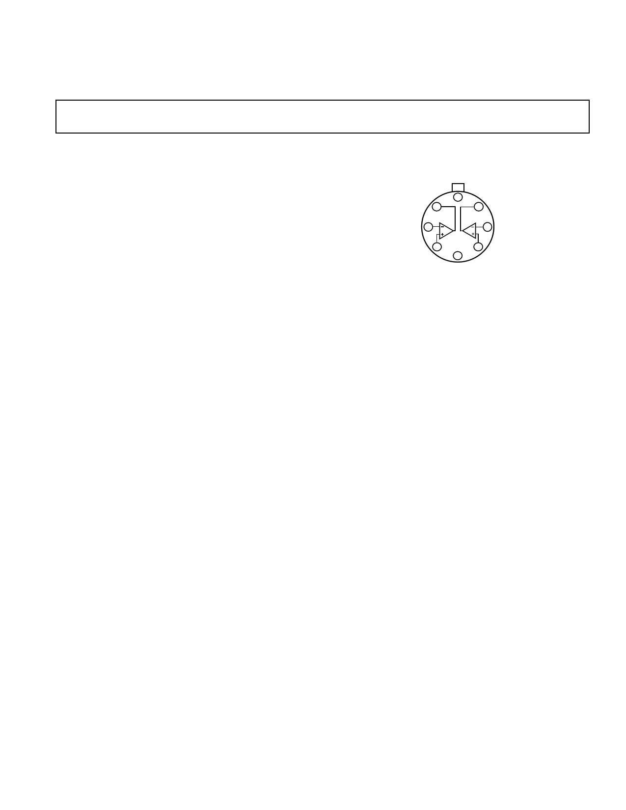
PIN CONFIGURATION
AMPLIFIER NO. 1
+V
AMPLIFIER NO. 2
8
OUTPUT 1
7 OUTPUT
INVERTING 2
INPUT
NONINVERTING 3
INPUT
TOP
VIEW
4
6 INVERTING
INPUT
5 NONINVERTING
INPUT
NOTE:
–V
PIN 4 CONNECTED TO CASE
PRODUCT DESCRIPTION
The AD644 is a pair of matched high speed monolithic FET in-
put operational amplifiers fabricated with the most advanced bi-
polar, JFET and laser-trimming technologies. The AD644 offers
matched bias currents that are significantly lower than currently
available monolithic dual BiFET operational amplifiers: 35 pA
max, matched to 25 pA for the AD644K and L, 75 pA max
matched to 35 pA for the AD644J and S. In addition, the offset
voltage is laser trimmed to less than 0.5 mV, and matched to
0.25 mV for the AD644L, 1.0 mV and matched to 0.5 mV for
the AD644K, utilizing Analog Devices’ laser-wafer trimming
(LWT) process.
The tight matching and temperature tracking between the op-
erational amplifiers is achieved by ion-implanted JFETs and
laser-wafer trimming. Ion-implantation permits the fabrication
of precision, matched JFETs on a monolithic bipolar chip. This
process optimizes the ability to produce matched amplifiers
which have lower initial bias currents than other popular BiFET
op amps. Laser-wafer trimming each amplifier’s input offset
voltage assures tight initial match and superior IC processing
guarantees offset voltage tracking over the temperature range.
The AD644 is recommended for applications in which both
excellent ac and dc performance is required. The matched am-
plifiers provide a low cost solution to true wideband instrumen-
tation amplifiers, low dc drift active filters and output amplifiers
for four quadrant multiplying D/A converters such as the
AD7541, 12-bit CMOS DAC.
The AD644 is available in four versions: the “J”, “K” and “L”
are specified over the 0°C to +70°C temperature range and the
“S” over the –55°C to +125°C operating temperature range.
All devices are packaged in the hermetically sealed, TO-99
metal can or available in chip form.
PRODUCT HIGHLIGHTS
1. The AD644 has tight side to side matching specifications to
ensure high performance without matching individual devices.
2. Analog Devices, unlike some manufacturers, specifies each
device for the maximum bias current at either input in the
warmed-up condition, thus assuring the user that the AD644
will meet its published specifications in actual use.
3. Laser-wafer-trimming reduces offset voltage to as low as
0.5 mV max matched side to side to 0.25 mV (AD644L),
thus eliminating the need for external nulling.
4. Improved bipolar and JFET processing on the AD644 result
in the lowest matched bias current available in a high speed
monolithic FET op amp.
5. Low voltage noise (2 µV p-p) and high open loop gain
enhance the AD644’s performance as a precision op amp.
6. The high slew rate (13.0 V/µs) and fast settling time to
0.01% (3.0 µs) make the AD644 ideal for D/A, A/D, sample-
hold circuits and dual high speed integrators.
7. Low harmonic distortion (0.0015%) and low crosstalk
(–124 dB) make the AD644 an ideal choice for stereo audio
applications.
8. The standard dual amplifier pin out allows the AD644 to
replace lower performance duals without redesign.
9. The AD644 is available in chip form.
REV. A
Information furnished by Analog Devices is believed to be accurate and
reliable. However, no responsibility is assumed by Analog Devices for its
use, nor for any infringements of patents or other rights of third parties
which may result from its use. No license is granted by implication or
otherwise under any patent or patent rights of Analog Devices.
One Technology Way, P.O. Box 9106, Norwood, MA 02062-9106, U.S.A.
Tel: 617/329-4700
Fax: 617/326-8703
1 page 
AD644
low pass filter formed by the 100 Ω series resistor and the load
capacitance, CL.
The low input bias current (35 pA), low noise, high slew rate
and high bandwidth characteristics of the AD644 make it suit-
able for electrometer applications such as photodiode preampli-
fiers and picoampere current-to-voltage converters. The use of
guarding techniques in printed circuit board layout and con-
struction is critical for achieving the ultimate in low leakage per-
formance that the AD644 can deliver. The input guarding
scheme shown in Figure 25 will minimize leakage as much as
possible. The same layout should be used on both sides of a
double side board. The guard ring is connected to a low imped-
ance potential at the same level as the inputs. High impedance
signal lines should not be extended for any unnecessary length
on a printed circuit; to minimize noise and leakage, such con-
ductors should be replaced by rigid shielded cables.
The fast settling time (3.0 µs to 0.01% for 20 V p-p step) and
low offset voltage make the AD644 an excellent choice as an
output amplifier for current output D/A converters such as the
AD7541. The upper trace of the oscilloscope photograph of Fig-
ure 23b shows the settling characteristics of the AD644. The
lower trace represents the input to Figure 23a. The AD644 has
been designed for fast settling to 0.01%, however, feedback
components, circuit layout and circuit design must be carefully
considered to obtain the optimum settling time.
Figure 25. Board Layout for Guarding Inputs
INPUT PROTECTION
The AD644 is guaranteed for a maximum safe input potential
equal to the power supply potential. The input stage design also
allows differential input voltages of up to ± 1 volt while main-
taining the full differential input resistance of 1012 Ω. This
makes the AD644 suitable for comparator situations employing
a direct connection to high impedance source.
Many instrumentation situations, such as flame detectors in gas
chromatographs, involve measurement of low level currents
from high voltage sources. In such applications, a sensor fault
condition may apply a very high potential to the input of the
current-to-voltage converting amplifier. This possibility necessi-
tates some form of input protection. Many electrometer type
devices, especially CMOS designs, can require elaborate Zener
protection schemes which often compromise overall performance.
The AD644 requires input protection only if the source is not
current-limited, and as such is similar to many JFET-input
designs. The failure mode would be overheating from excess
current rather than voltage breakdown. If the source is not
current-limited, all that is required is a resistor in series with the
affected input terminal so that the maximum overload current is
1.0 mA (for example, 100 kΩ for a 100 volt overload). This
simple scheme will cause no significant reduction in perfor-
mance and give complete overload protection. Figure 26 shows
proper connections.
The circuit in Figure 24 employs a 100 Ω isolation resistor
which enables the amplifier to drive capacitive loads exceeding
500 pF; the resistor effectively isolates the high frequency feed-
back from the load and stabilizes the circuit. Low frequency
feedback is returned to the amplifier summing junction via the
REV. A
–5–
Figure 26. AD644 Input Protection
5 Page | ||
| Páginas | Total 6 Páginas | |
| PDF Descargar | [ Datasheet AD644.PDF ] | |
Hoja de datos destacado
| Número de pieza | Descripción | Fabricantes |
| AD640 | DC-Coupled Demodulating 120 MHz Logarithmic Amplifier | Analog Devices |
| AD6402 | IF Transceiver Subsystem | Analog Devices |
| AD641 | 250 MHz Demodulating Logarithmic Amplifier | Analog Devices |
| AD6411 | DECT RF Transceiver | Analog Devices |
| Número de pieza | Descripción | Fabricantes |
| SLA6805M | High Voltage 3 phase Motor Driver IC. |
Sanken |
| SDC1742 | 12- and 14-Bit Hybrid Synchro / Resolver-to-Digital Converters. |
Analog Devices |
|
DataSheet.es es una pagina web que funciona como un repositorio de manuales o hoja de datos de muchos de los productos más populares, |
| DataSheet.es | 2020 | Privacy Policy | Contacto | Buscar |