|
|
|
PDF ADP3810AR-42 Data sheet ( Hoja de datos )
| Número de pieza | ADP3810AR-42 | |
| Descripción | Secondary Side/ Off-Line Battery Charger Controllers | |
| Fabricantes | Analog Devices | |
| Logotipo | ||
Hay una vista previa y un enlace de descarga de ADP3810AR-42 (archivo pdf) en la parte inferior de esta página. Total 16 Páginas | ||
|
No Preview Available !
a
FEATURES
Programmable Charge Current
High Precision Battery Voltage Limit
Precision 2.000 V Reference
Low Voltage Drop Current Sense: 300 mV Full Scale
Full Operation in Shorted and Open Battery Conditions
Drives Diode-Side of Optocoupler
Wide Operating Supply Range: 2.7 V to 16 V
Undervoltage Lockout
SO-8 Package
ADP3810
Internal Precision Voltage Divider for Battery Sense
Four Final Battery Voltage Options Available: 4.2 V,
8.4 V, 12.6 V, 16.8 V
ADP3811
Adjustable Final Battery Voltage
APPLICATIONS
Battery Charger Controller for:
LiIon Batteries (ADP3810)
NiCad, NiMH Batteries (ADP3811)
GENERAL DESCRIPTION
The ADP3810 and ADP3811 combine a programmable current
limit with a battery voltage limit to provide a constant current,
constant voltage battery charger controller. In secondary side,
Secondary Side, Off-Line
Battery Charger Controllers
ADP3810/ADP3811
off-line applications, the output directly drives the diode side of
an optocoupler to give isolated feedback control of a primary
side PWM. The circuitry includes two gain (gm) stages, a preci-
sion 2.0 V reference, a control input buffer, an Undervoltage
Lock Out (UVLO) comparator, an output buffer and an over-
voltage comparator.
The current limit amplifier senses the voltage drop across an
external sense resistor to control the average current for charg-
ing a battery. The voltage drop can be adjusted from 25 mV
to 300 mV, giving a charging current limit from 100 mA to
1.2 amps with a 0.25 Ω sense resistor. An external dc voltage
on the VCTRL input sets the voltage drop. Because this input
is high impedance, a filtered PWM output can be used to set
the voltage.
As the battery voltage approaches its voltage limit, the voltage
sense amplifier takes over to maintain a constant battery volt-
age. The two amplifiers essentially operate in an “OR” fash-
ion. Either the current is limited, or the voltage is limited.
The ADP3810 has internal thin-film resistors that are trimmed
to provide a precise final voltage for LiIon batteries. Four volt-
age options are available, corresponding to 1-4 LiIon cells as
follows: 4.2 V, 8.4 V, 12.6 V and 16.8 V.
The ADP3811 omits these resistors allowing any battery volt-
age to be programmed with external resistors.
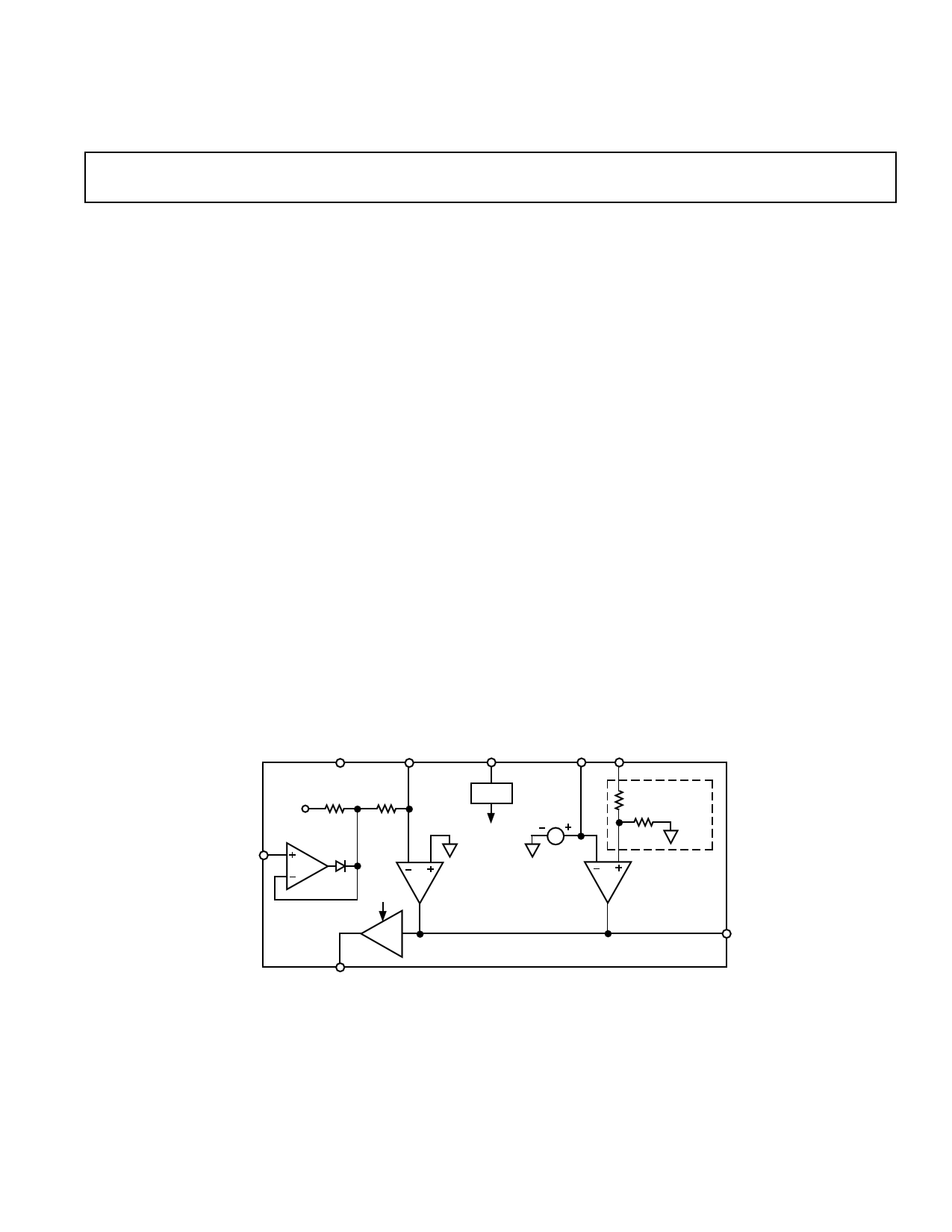
GND
FUNCTIONAL BLOCK DIAGRAM
VCS
VCC
VREF VSENSE
VREF
1.5MΩ
80kΩ
VCTRL
UVLO
GM
UVLO
UVLO
VREF
GM1 ADP3810/
ADP3811
R1
ADP3810
ONLY
R2
GM 2
COMP
OUT
REV. 0
Information furnished by Analog Devices is believed to be accurate and
reliable. However, no responsibility is assumed by Analog Devices for its
use, nor for any infringements of patents or other rights of third parties
which may result from its use. No license is granted by implication or
otherwise under any patent or patent rights of Analog Devices.
One Technology Way, P.O. Box 9106, Norwood, MA 02062-9106, U.S.A.
Tel: 617/329-4700 World Wide Web Site: http://www.analog.com
Fax: 617/326-8703
© Analog Devices, Inc., 1996
1 page 
100
80
60
40
20
0
–20
–40
–60
10
GAIN
CCOMP = 0.01µF
TA = +25°C
VCC = +10V
PHASE
100 1k 10k 100k
FREQUENCY – Hz
0
45
90
135
180
225
1M
Figure 11. GM2 Open-Loop Gain and
Phase vs. Frequency
1.0
VCC = +10V
0.5
0
–0.5
–1.0
–1.5
–50
–25 0
25 50 75
TEMPERATURE – °C
100
Figure 12. ADP3810 Voltage Sense
Accuracy vs. Temperature
1.0
VCC = +10V
0.5
0
–0.5
–1.0
–1.5
–50
–25 0 25 50 75
TEMPERATURE – °C
100
Figure 14. ADP3811 GM2 Offset vs.
Temperature
1.0
TA = +25°C
0.5
0
–0.5
–1.0
–1.5
0
36
9 12 15
SUPPLY VOLTAGE, VCC – Volts
18
Figure 15. ADP3811, GM2 Offset
vs. VCC
ADP3810/ADP3811
1.0
TA = +25°C
0.5
0
–0.5
–1.0
–1.5
0
36
9 12 15
SUPPLY VOLTAGE, VCC – Volts
18
Figure 13. ADP3810 Voltage Sense
Accuracy vs. VCC
2.5
VCC = +10V
2.0
1.5
1.0
0.5
0
–50 –25 0 25 50 75
TEMPERATURE – °C
100
Figure 16. ADP3811 VSENSE Bias
Current vs. Temperature
2.5
TA = +25°C
2.0
1.5
1.0
0.5
0
03
6 9 12 15 18
SUPPLY VOLTAGE, VCC – Volts
Figure 17. ADP3811 VSENSE Bias
Current vs. VCC
120
VCC = +10V
100 TA = +25°C
80
60
40
20
0
5.0 5.2 5.4 5.6 5.8 6.0 6.2 6.4 6.6 6.8 7.0
VOV% – %
Figure 18. Overvoltage Comparator
Distribution (VOV%)
12
VCC = +10V
10
8
6
4
2
–50 –25 0 25 50 75
TEMPERATURE – °C
100
Figure 19. Overvoltage Comparator
Threshold (VOV%) vs. Temperature
REV. 0
–5–
5 Page 
ADP3810/ADP3811
100
90
10V
TA = +25؇C
VIN = 220VAC
VCTRL = 1V
6V
10
0%
0V
2V/DIV
50msec/DIV
Figure 27. Output Voltage Transient Response to Battery
Connect/Disconnect
NONISOLATED TOPOLOGIES
Buck Switching Regulators
The ADP3810/ADP3811 and the ADP1148 can be combined
to create a high efficiency buck regulator battery charger as
shown in Figure 28. The ADP1148 is a high efficiency, synchro-
nous, step-down regulator that controls two external MOSFETs
as shown. Similar to the previous flyback circuit, the ADP3810
controls the average charge current and the final battery voltage,
and the ADP1148 controls the cycle by cycle current. The fol-
lowing discussion explains the functionality of the circuit but
does not go into detail on the ADP1148. For more information,
the ADP1148 data sheet details the operation of the device and
gives formulas for choosing the external components.
The resistor RSENSE sets the cycle by cycle current limit to 1.5 A,
which is far enough above the 1 A average current of the
ADP3810 loop to avoid interfering but still provides a safe
maximum current to protect the external components. The
ADP3810 uses a 0.25 Ω resistor, RCS, to sense the battery cur-
rent. As before, a 20 kΩ resistor is needed between RCS and the
VCS input of the ADP3810. The RC network from VCS to ground
performs the dual function of filtering and compensation.
The voltage loop directly senses the battery voltage. Since the
ADP3810 is used in this circuit instead of the ADP3811, VSENSE
is connected directly to the battery. The internal resistors set the
battery voltage to 8.4 V in this case. Of course, other voltage
options could be used, or the ADP3811 could be substituted
with external resistors for a user set voltage. Notice the two
grounds in the circuit. One ground is for the high current re-
turn to the VIN source and the other ground for the ADP3810
circuitry. RCS separates the two grounds, and it is important to
keep them separate as shown.
The adjustable version of the ADP1148 is used in this circuit in-
stead of a fixed output version. The output voltage is fed back
into the VFB pin, which is set to regulate at VBAT MAX + 0.5 V.
Doing so provides a secondary, higher voltage limit without
interfering with normal circuit operation. The control output of
the ADP3810 is connected through a 560 Ω resistor to the
SENSE+ input of the ADP1148. The current, IOUT, adjusts the
dc level on the SENSE+ pin, which is added to the current
ramp across RSENSE. Higher IOUT increases the voltage on
SENSE+ and reduces the duty cycle of the 1148, giving nega-
tive feedback.
The circuit as shown can quickly and safely charge LiIon batter-
ies while maintaining high efficiency. The efficiency of the
ADP1148 is only degraded slightly by the addition of the
ADP3810 and external circuitry. The 1.5 mA of supply current
lowers the overall efficiency by approximately 1%–2% for maxi-
mum output current. The 0.25 Ω sense resistor further lowers
the efficiency due to the I2 × RCS power loss at high output cur-
rents. See the efficiency discussion in the ADP1148 data sheet
for more information.
Linear Regulator
A third charging circuit is shown in Figure 29. In this case, the
switching supply is replaced with a linear regulator. The ADP3811
drives the gate of an N-channel MOSFET using an external
2N3904. As before, the ADP3811 senses the charge current
through a 0.25 Ω resistor. When the current increases above the
limit, the internal GM amplifier causes the output to go high.
This puts more voltage across R8, increasing the current in Q1.
As the current increases, the gate of M1 is pulled lower, reduc-
ing the gate to source voltage and decreasing the charge current
to complete the feedback loop. Because the ADP3811 has a
current output, an external 1 kΩ resistor is needed from the
OUT pin to ground in order to convert the current to a voltage.
+VIN
0.1µF
VREF
VCTRL
(0V TO 1V)
0.1µF
VSENSE
VCC
OUT
VREF ADP3810
VCTRL
VCS
REF & CTRL
RTN
VIN
RTN
0.1µF
GND
COMP
RC1
2kΩ
CC1
1µF
* COILTRONICS CTX-68-4
** KRL SL-1-C1-0R068J
1µF
0V = NORMAL
>1.5V = SHUTDOWN
RC2
560Ω
CC2
220nF
20kΩ
CT
68pF
75kΩ
VIN
P DRIVE
SHUTDOWN
VFB
SENSE+
ADP1148
SENSE–
10
kΩ
CT
S GND
N DRIVE
P GND
560Ω
CIN
100µF
P CH
IRF7204
L*
62µH
RSENSE**
50 mΩ VBAT
1000pF
N CH
IRF7403
100Ω
100Ω
COUT
220µF
D1
10BQ040
BATTERY
RCS
0.25Ω
Figure 28. High Efficiency Buck Battery Charger
REV. 0
–11–
11 Page | ||
| Páginas | Total 16 Páginas | |
| PDF Descargar | [ Datasheet ADP3810AR-42.PDF ] | |
Hoja de datos destacado
| Número de pieza | Descripción | Fabricantes |
| ADP3810AR-42 | Secondary Side/ Off-Line Battery Charger Controllers | Analog Devices |
| Número de pieza | Descripción | Fabricantes |
| SLA6805M | High Voltage 3 phase Motor Driver IC. |
Sanken |
| SDC1742 | 12- and 14-Bit Hybrid Synchro / Resolver-to-Digital Converters. |
Analog Devices |
|
DataSheet.es es una pagina web que funciona como un repositorio de manuales o hoja de datos de muchos de los productos más populares, |
| DataSheet.es | 2020 | Privacy Policy | Contacto | Buscar |