|
|
|
PDF 16F84A Data sheet ( Hoja de datos )
| Número de pieza | 16F84A | |
| Descripción | 18-pin Enhanced Flash/EEPROM 8-Bit Microcontroller | |
| Fabricantes | Microchip Technology | |
| Logotipo | ||
Hay una vista previa y un enlace de descarga de 16F84A (archivo pdf) en la parte inferior de esta página. Total 68 Páginas | ||
|
No Preview Available !
M
PIC16F84A
18-pin Enhanced Flash/EEPROM 8-Bit Microcontroller
Devices Included in this Data Sheet:
• PIC16F84A
• Extended voltage range device available
(PIC16LF84A)
High Performance RISC CPU Features:
• Only 35 single word instructions to learn
• All instructions single cycle except for program
branches which are two-cycle
• Operating speed: DC - 20 MHz clock input
DC - 200 ns instruction cycle
• 1024 words of program memory
• 68 bytes of data RAM
• 64 bytes of data EEPROM
• 14-bit wide instruction words
• 8-bit wide data bytes
• 15 special function hardware registers
• Eight-level deep hardware stack
• Direct, indirect and relative addressing modes
• Four interrupt sources:
- External RB0/INT pin
- TMR0 timer overflow
- PORTB<7:4> interrupt on change
- Data EEPROM write complete
Peripheral Features:
• 13 I/O pins with individual direction control
• High current sink/source for direct LED drive
- 25 mA sink max. per pin
- 25 mA source max. per pin
• TMR0: 8-bit timer/counter with 8-bit
programmable prescaler
Special Microcontroller Features:
• 1000 erase/write cycles Enhanced Flash program
memory
• 1,000,000 typical erase/write cycles EEPROM data
memory
• EEPROM Data Retention > 40 years
• In-Circuit Serial Programming (ICSP™) - via two
pins
• Power-on Reset (POR), Power-up Timer (PWRT),
Oscillator Start-up Timer (OST)
• Watchdog Timer (WDT) with its own on-chip RC
oscillator for reliable operation
• Code-protection
• Power saving SLEEP mode
• Selectable oscillator options
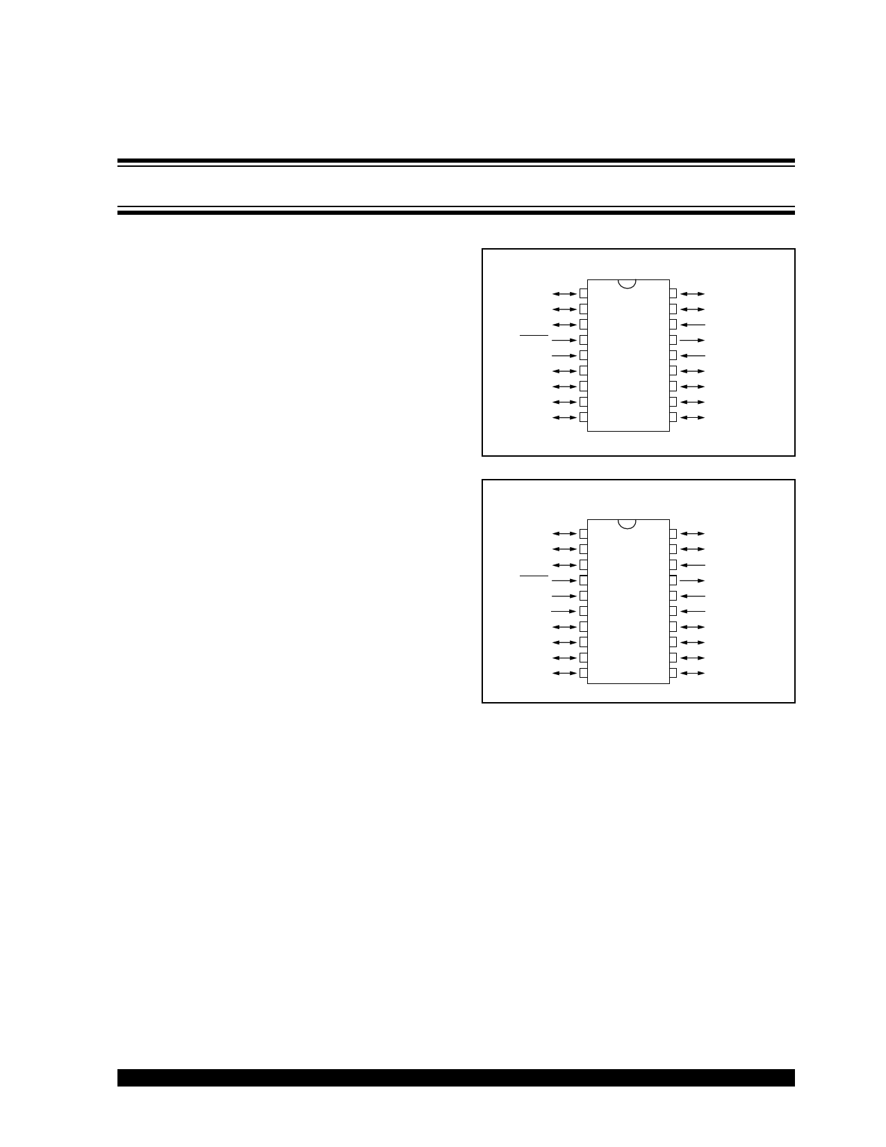
Pin Diagrams
PDIP, SOIC
RA2
RA3
RA4/T0CKI
MCLR
VSS
RB0/INT
RB1
RB2
RB3
•1
2
3
4
5
6
7
8
9
18
17
16
15
14
13
12
11
10
RA1
RA0
OSC1/CLKIN
OSC2/CLKOUT
VDD
RB7
RB6
RB5
RB4
RA2
RA3
RA4/T0CKI
MCLR
VSS
VSS
RB0/INT
RB1
RB2
RB3
SSOP
•1 20
2 19
3 18
4 17
5 16
6 15
7 14
8 13
9 12
10 11
RA1
RA0
OSC1/CLKIN
OSC2/CLKOUT
VDD
VDD
RB7
RB6
RB5
RB4
CMOS Enhanced Flash/EERPOM Technology:
• Low-power, high-speed technology
• Fully static design
• Wide operating voltage range:
- Commercial: 2.0V to 5.5V
- Industrial: 2.0V to 5.5V
• Low power consumption:
- < 2 mA typical @ 5V, 4 MHz
- 15 µA typical @ 2V, 32 kHz
- < 0.5 µA typical standby current @ 2V
© 1998 Microchip Technology Inc.
Preliminary
DS35007A-page 1
1 page 
2.0 MEMORY ORGANIZATION
There are two memory blocks in the PIC16F84A.
These are the program memory and the data memory.
Each block has its own bus, so that access to each
block can occur during the same oscillator cycle.
The data memory can further be broken down into the
general purpose RAM and the Special Function
Registers (SFRs). The operation of the SFRs that
control the “core” are described here. The SFRs used
to control the peripheral modules are described in the
section discussing each individual peripheral module.
The data memory area also contains the data
EEPROM memory. This memory is not directly mapped
into the data memory, but is indirectly mapped. That is,
an indirect address pointer specifies the address of the
data EEPROM memory to read/write. The 64 bytes of
data EEPROM memory have the address range
0h-3Fh. More details on the EEPROM memory can be
found in Section 5.0.
Additional information on device memory may be found
in the PICmicro™ Mid-Range Reference Manual,
(DS33023).
2.1 Program Memory Organization
The PIC16FXX has a 13-bit program counter capable
of addressing an 8K x 14 program memory space.
For the PIC16F84A, the first 1K x 14 (0000h-03FFh)
are physically implemented (Figure 2-1). Accessing a
location above the physically implemented address will
cause a wraparound. For example, for locations 20h,
420h, 820h, C20h, 1020h, 1420h, 1820h, and 1C20h
will be the same instruction.
The reset vector is at 0000h and the interrupt vector is
at 0004h.
PIC16F84A
FIGURE 2-1: PROGRAM MEMORY MAP
AND STACK - PIC16F84A
PC<12:0>
CALL, RETURN
13
RETFIE, RETLW
Stack Level 1
•••
Stack Level 8
Reset Vector
0000h
Peripheral Interrupt Vector 0004h
3FFh
1FFFh
© 1998 Microchip Technology Inc.
Preliminary
DS35007A-page 5
5 Page 
2.3 PCL and PCLATH
The program counter (PC) specifies the address of the
instruction to fetch for execution. The PC is 13 bits
wide. The low byte is called the PCL register. This reg-
ister is readable and writable. The high byte is called
the PCH register. This register contains the PC<12:8>
bits and is not directly readable or writable. All updates
to the PCH register go through the PCLATH register.
2.3.1 STACK
The stack allows a combination of up to 8 program calls
and interrupts to occur. The stack contains the return
address from this branch in program execution.
Midrange devices have an 8 level deep x 13-bit wide
hardware stack. The stack space is not part of either
program or data space and the stack pointer is not
readable or writable. The PC is PUSHed onto the stack
when a CALL instruction is executed or an interrupt
causes a branch. The stack is POPed in the event of a
RETURN, RETLW or a RETFIE instruction execution.
PCLATH is not modified when the stack is PUSHed or
POPed.
After the stack has been PUSHed eight times, the ninth
push overwrites the value that was stored from the first
push. The tenth push overwrites the second push (and
so on).
PIC16F84A
2.4 Indirect Addressing; INDF and FSR
Registers
The INDF register is not a physical register. Address-
ing INDF actually addresses the register whose
address is contained in the FSR register (FSR is a
pointer). This is indirect addressing.
EXAMPLE 2-1: INDIRECT ADDRESSING
• Register file 05 contains the value 10h
• Register file 06 contains the value 0Ah
• Load the value 05 into the FSR register
• A read of the INDF register will return the value of
10h
• Increment the value of the FSR register by one
(FSR = 06)
• A read of the INDF register now will return the
value of 0Ah.
Reading INDF itself indirectly (FSR = 0) will produce
00h. Writing to the INDF register indirectly results in a
no-operation (although STATUS bits may be affected).
A simple program to clear RAM locations 20h-2Fh
using indirect addressing is shown in Example 2-2.
EXAMPLE 2-2:
NEXT
CONTINUE
movlw
movwf
clrf
incf
btfss
goto
:
HOW TO CLEAR RAM
USING INDIRECT
ADDRESSING
0x20 ;initialize pointer
FSR ; to RAM
INDF ;clear INDF register
FSR ;inc pointer
FSR,4 ;all done?
NEXT ;NO, clear next
;YES, continue
An effective 9-bit address is obtained by concatenating
the 8-bit FSR register and the IRP bit (STATUS<7>), as
shown in Figure 2-1. However, IRP is not used in the
PIC16F84A.
© 1998 Microchip Technology Inc.
Preliminary
DS35007A-page 11
11 Page | ||
| Páginas | Total 68 Páginas | |
| PDF Descargar | [ Datasheet 16F84A.PDF ] | |
Hoja de datos destacado
| Número de pieza | Descripción | Fabricantes |
| 16F84 | 18-pin Flash/EEPROM 8-Bit Microcontrollers | Microchip Technology |
| 16F84A | 18-pin Flash/EEPROM 8-Bit Microcontrollers | Microchip Technology |
| 16F84A | 18-pin Enhanced Flash/EEPROM 8-Bit Microcontroller | Microchip Technology |
| 16F84A | 18-pin Enhanced Flash/EEPROM 8-Bit Microcontroller | Microchip Technology |
| Número de pieza | Descripción | Fabricantes |
| SLA6805M | High Voltage 3 phase Motor Driver IC. |
Sanken |
| SDC1742 | 12- and 14-Bit Hybrid Synchro / Resolver-to-Digital Converters. |
Analog Devices |
|
DataSheet.es es una pagina web que funciona como un repositorio de manuales o hoja de datos de muchos de los productos más populares, |
| DataSheet.es | 2020 | Privacy Policy | Contacto | Buscar |