|
|
|
PDF TSF18N50MR Data sheet ( Hoja de datos )
| Número de pieza | TSF18N50MR | |
| Descripción | N-Channel MOSFET | |
| Fabricantes | Truesemi | |
| Logotipo | ||
Hay una vista previa y un enlace de descarga de TSF18N50MR (archivo pdf) en la parte inferior de esta página. Total 7 Páginas | ||
|
No Preview Available !
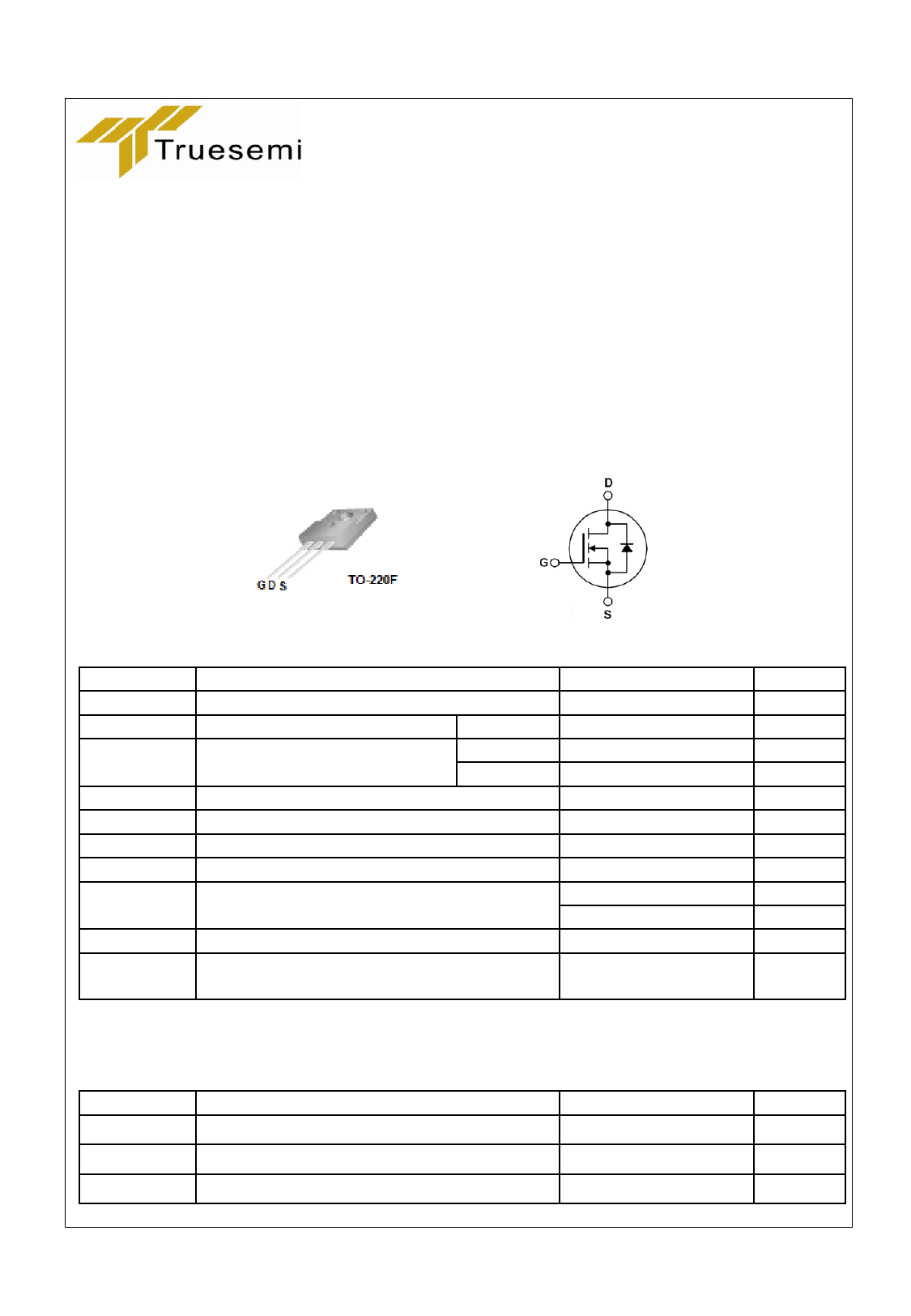
TSF18N50MR
500V N-Channel MOSFET
General Description
This Power MOSFET is produced using Truesemi‘s
advanced planar stripe DMOS technology.
This advanced technology has been especially tailored to
minimize on-state resistance, provide superior switching
performance, and withstand high energy pulse in the
avalanche and commutation mode. These devices are well
suited for high efficiency switched mode power supplies,
active power factor correction based on half bridge
topology.
Features
• 18.0A,500V,Max.RDS(on)=0.31 Ω @ VGS =10V
• Low gate charge(typical 45nC)
• High ruggedness
• Fast switching
• 100% avalanche tested
• Improved dv/dt capability
Absolute Maximum Ratings TC=25℃ unless otherwise specified
Symbol
VDSS
VGS
ID
IDM
EAS
EAR
dv/dt
PD
TJ, TSTG
TL
Parameter
Drain-Source Voltage
Gate-Source Voltage
Drain Current
Pulsed Drain Current
TC = 25℃
TC = 100℃
(Note 1)
Single Pulsed Avalanche Energy
(Note 2)
Repetitive Avalanche Energy
(Note 1)
Peak Diode Recovery dv/dt
(Note 3)
Power Dissipation (TC = 25℃)
-Derate above 25℃
Operating and Storage Temperature Range
Maximum lead temperature for soldering purposes,
1/8” from case for 5 seconds
Value
500
± 30
18*
10.8*
72*
945
23.5
4.5
38.5
0.3
-55 to +150
300
* Drain current limited by maximum junction temperature.
Thermal Resistance Characteristics
Symbol
RθJC
RθCS
RθJA
Parameter
Thermal Resistance,Junction-to-Case
Thermal Resistance,Case-to-Sink Typ.
Thermal Resistance,Junction-to-Ambient
Value
3.3
--
62.5
Units
V
V
A
A
A
mJ
mJ
V/ns
W
W/℃
℃
℃
Units
℃/W
℃/W
℃/W
© 2015 Truesemi Semiconductor Corporation
Ver.B1
www.truesemi.com
1 page 
Fig 12. Gate Charge Test Circuit & Waveform
Same Type
50KΩ as DUT
12V 200nF
300nF
VGS
10V
Qg
VGS
VDS
Qgs Qgd
DUT
3mA
Charge
10V
10V
Fig 13. Resistive Switching Test Circuit & Waveforms
VDS
RG
RL
VDD
( 0.5 rated VDS )
DUT
VDS
90%
10%
Vin
td(on)
tr
t on
td(off)
tf
t off
Fig 14. Unclamped Inductive Switching Test Circuit & Waveforms
VDS
ID
RG
L
VDD
BVDSS
IAS
EAS =
--1--
2
LL IAS2
ID (t)
DUT
VDD
tp
VDS (t)
Time
© 2015 Truesemi Semiconductor Corporation
Ver.B1
www.truesemi.com
5 Page | ||
| Páginas | Total 7 Páginas | |
| PDF Descargar | [ Datasheet TSF18N50MR.PDF ] | |
Hoja de datos destacado
| Número de pieza | Descripción | Fabricantes |
| TSF18N50M | N-Channel MOSFET | Truesemi |
| TSF18N50MR | N-Channel MOSFET | Truesemi |
| Número de pieza | Descripción | Fabricantes |
| SLA6805M | High Voltage 3 phase Motor Driver IC. |
Sanken |
| SDC1742 | 12- and 14-Bit Hybrid Synchro / Resolver-to-Digital Converters. |
Analog Devices |
|
DataSheet.es es una pagina web que funciona como un repositorio de manuales o hoja de datos de muchos de los productos más populares, |
| DataSheet.es | 2020 | Privacy Policy | Contacto | Buscar |