|
|
|
PDF RSL10 Data sheet ( Hoja de datos )
| Número de pieza | RSL10 | |
| Descripción | Ultra-Low-Power Multi-protocol Bluetooth 5 System-on-Chip | |
| Fabricantes | ON Semiconductor | |
| Logotipo | ||
Hay una vista previa y un enlace de descarga de RSL10 (archivo pdf) en la parte inferior de esta página. Total 18 Páginas | ||
|
No Preview Available !
RSL10
Product Preview
Ultra-Low-Power
Multi-protocol Bluetooth 5
System-on-Chip (SoC)
Introduction
RSL10 is an ultra−low−power, highly flexible multi−protocol
2.4 GHz radio specifically designed for use in high−performance
wearable and medical applications. With its ARM® Cortex®−M3
Processor and LPDSP32 DSP core, RSL10 supports Bluetooth low
energy technology and 2.4 GHz proprietary protocol stacks, without
sacrificing power consumption.
Key Features
• Rx Sensitivity (Bluetooth Low Energy Technology Mode, 1 Mbps):
−94 dBm
• Data Rate: 62.5 to 2000 kbps
• Transmitting Power: −17 to +6 dBm
• Peak Rx Current = 5.6 mA (1.25 V VBAT)
• Peak Rx Current = 3.0 mA (3 V VBAT)
• Peak Tx Current (0 dBm) = 8.9 mA (1.25 V VBAT)
• Peak Tx Current (0 dBm) = 4.6 mA (3 V VBAT)
• Bluetooth 5 Certified with 2 Mbps Support
• ARM Cortex−M3 processor clocked up to 48 MHz
• LPDSP32 for Audio CODEC
• Supply Voltage Range: 1.1 − 3.6 V
• Current Consumption (1.25 V VBAT):
♦ Deep Sleep, IO wake−up: 50 nA
♦ Deep Sleep, 8 kB RAM retention: 300 nA
♦ Audio Streaming at 7 kHz audio BW: 1.8 mA RX, 1.8 mA TX
• Current Consumption (3 V VBAT):
♦ Deep Sleep, IO wake−up: 25 nA
♦ Deep Sleep, 8 kB RAM retention: 100 nA
♦ Audio Streaming at 7 kHz audio BW: 0.9 mA RX, 0.9 mA TX
• 384 kB of flash memory
• Highly−integrated System−on−Chip (SoC)
• Supports FOTA (Firmware Over−The−Air) updates
This document contains information on a product under development.
ON Semiconductor reserves the right to change or discontinue this
product without notice.
This document, and the information contained herein, is CONFIDENTIAL AND
PROPRIETARY and the property of Semiconductor Components Industries,
LLC., dba ON Semiconductor. It shall not be used, published, disclosed or
disseminated outside of the Company, in whole or in part, without the written
permission of ON Semiconductor. Reverse engineering of any or all of the
information contained herein is strictly prohibited.
E 2017, SCILLC. All Rights Reserved.
www.onsemi.com
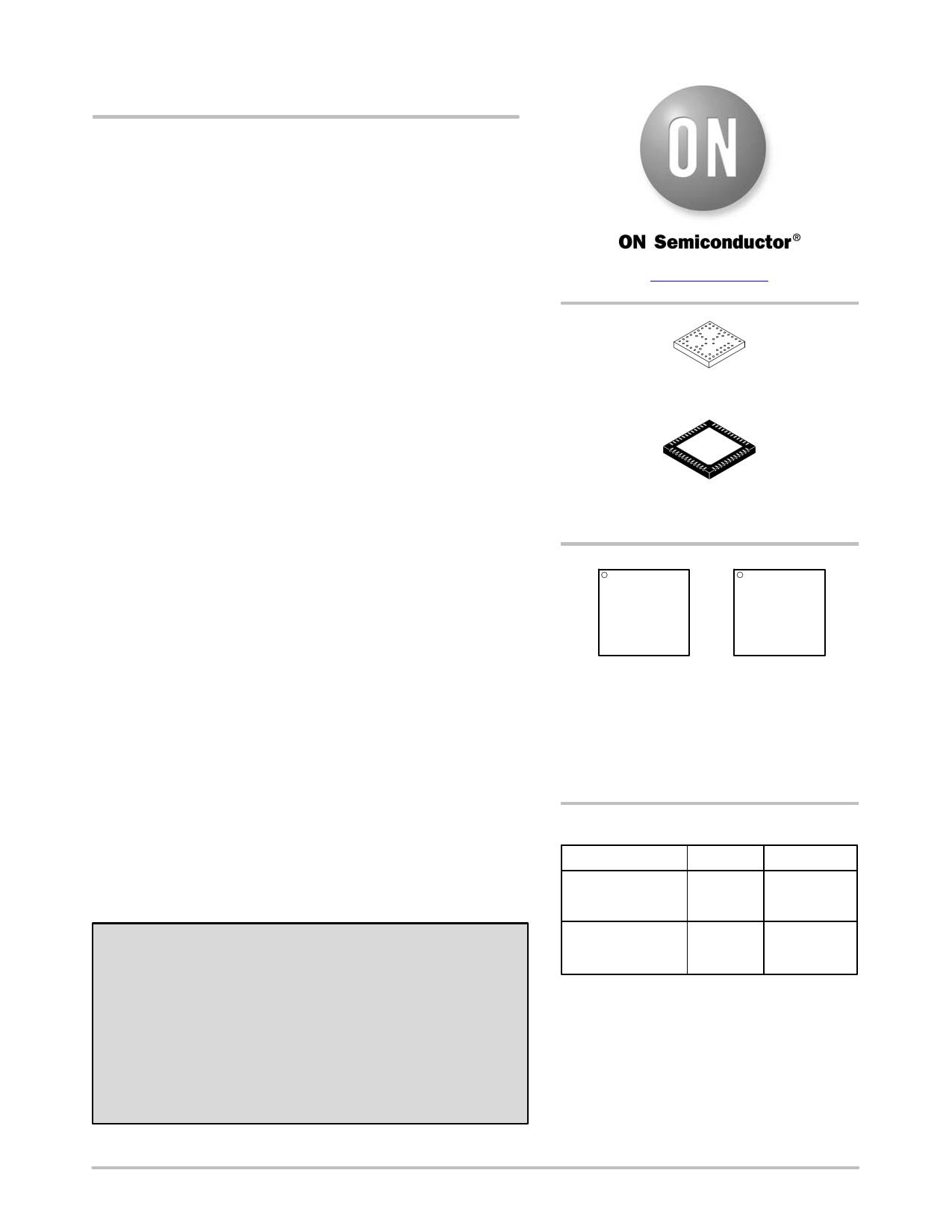
WLCSP51
CASE 567MT
1 48
QFN48
CASE 485BA
RSL10
AWLYYWWG
(QFN48)
RSL10
AWLYWW
G
(WLCSP51)
XXXXXX = Specific Device Code
A = Assembly Location
WL = Wafer Lot
Y or YY = Year
WW = Work Week
G or G = Pb−Free Package
ORDERING INFORMATION
Device
Package Shipping†
NCH−RSL10−
101WC51−ABG
(Note 1)
WLCSP51 5000 / Tape &
(Pb−Free)
Reel
NCH−RSL10−
101Q48−ABG
(Note 2)
QFN48 5000 / Tape &
(Pb−Free)
Reel
†For information on tape and reel specifications,
including part orientation and tape sizes, please
refer to our Tape and Reel Packaging Specification
Brochure, BRD8011/D.
1. WLCSP version: production ready: May 2017
2. QFN48 version: production ready: July 2017
© Semiconductor Components Industries, LLC, 2016
February, 2017 − Rev. P4
1
Publication Order Number:
RSL10/D
1 page 
RSL10
Table 2. ELECTRICAL PERFORMANCE SPECIFICATIONS
Unless otherwise noted, production tests are performed at 25°C at VBAT = VDDO = 1.25 V.
Description
Symbol
Conditions
INTERNALLY GENERATED VDDRF: Radio Front end supply voltage
Supply voltage: trimming
step
VDDRFSTEP
INTERNALLY GENERATED VDDPA: Radio Power Amplifier Supply Voltage
Supply voltage: operating
range
VDDPA
Supply voltage: trimming
range
VDDPARANGE
Supply voltage: trimming
step
VDDPASTEP
INDUCTIVE BUCK DC−DC CONVERTER
VBAT range when the DC−
DC converter is active
(Note 7)
DCDC
IN_RANGE
VBAT range when the LDO
is active
Output voltage: trimming
range
Supply voltage: trimming
step
LDO
IN_RANGE
DCDC
OUT_RANGE
DCDCSTEP
POWER−ON RESET
POR voltage
VBATPOR
RADIO FRONT−END: General Specifications
RF input impedance
Input reflection coefficient
Data rate FSK / MSK /
GFSK
Zin
S11
RFSK
Single ended
All channels
OQPSK as MSK
Data rate 4−FSK
On−air data rate
bps GFSK
RADIO FRONT−END: Crystal and Clock Specifications
Xtal frequency
Equiv. series Res.
Differential equivalent load
capacitance
FXTAL
ESRXTAL
CLXTAL
Fundamental
Settling time
RADIO FRONT−END: Synthesizer Specifications
Frequency range
RX frequency step
FRF Supported carrier frequencies
RX Mode frequency synthesizer resolution
TX frequency step
TX Mode frequency synthesizer resolution
PLL Settling time, RX
tPLL_RX
RX Mode
PLL Settling time, TX
tPLL_TX
TX mode, BLE modulation
RADIO FRONT−END: Receive Mode Specifications
Current consumption at
1 Mbps, VBAT = 1.25 V
Current consumption at
2 Mbps, VBAT = 1.25 V
IBATRFRX
IBATRFRX
VDDRF =1.1 V, 100% duty cycle
VDDRF =1.1 V, 100% duty cycle
Min Typ
Max
− 10
−
1.05 1.6
1.05
− 10
1.68
1.68
−
1.4 3.6
1.1
1.0 1.2
− 10
3.6
1.32
−
0.4 0.8
1.0
− 50
−−
62.5 1000
−−
250
−
−8
3000
4000
2000
48
20 −
80
68
10
− 0.5
1.5
2360
−
−
−
−
−
−
−
15
5
2500
100
600
25
10
− 5.6
− 6.2
−
−
Units
mV
V
V
mV
V
V
V
mV
V
W
dB
kbps
kbps
kbps
MHz
W
pF
ms
MHz
Hz
Hz
ms
ms
mA
mA
www.onsemi.com
5
5 Page 
RSL10
Table 6. CHIP INTERFACE SPECIFICATIONS RSL10 has a total of 51 pads. Descriptions of these pads are given in Table X.
Pad Name
Description
Power
Domain
Pad #,
I/O A/D Pull WLCSP
Pad #,
QFN48
NRESET
Reset pin
VDDO
I DU
L9
16
WAKEUP
Wake−up pin for power modes
IA
L8 15
VDDC
LDO output for Core logic voltage supply
I/O P
H6 19
VDDM
LDO output for memories voltage supply
I/O P
F4 21
VDDO
Digital I/O voltage supply
I/O P
B4 36
VSSD
Digital ground pad for I/O
I/O P
F3, D6, F9 28, 35
VSS (*)
Substrate connection for the RF part
I/O P
B6 42
EXT_CLK
External clock input / Internal clock output
I/O D
U
F1
31
DIO[0]
Digital input output / LSAD (Low Speed ADC) 0
I/O A/D U/D
L4
18
DIO[1]
Digital input output / LSAD (Low Speed ADC) 1
I/O A/D U/D
L3
20
DIO[2]
Digital input output / LSAD (Low Speed ADC) 2
I/O A/D U/D
L2
23
DIO[3]
Digital input output / LSAD (Low Speed ADC) 3
I/O A/D U/D
L1
25
DIO[4]
Digital input output 4
I/O D U/D
K2
24
DIO[5]
Digital input output 5
I/O D U/D
K1
27
DIO[6]
Digital input output 6
I/O D U/D
J1
29
DIO[7]
Digital input output 7
I/O D U/D
H1
30
DIO[8]
Digital input output 8
I/O D U/D
G2
26
DIO[9]
Digital input output 9
I/O D U/D
E2
22
DIO[10]
Digital input output 10
I/O D U/D
D1
32
DIO[11]
Digital input output 11
I/O D U/D
B2
38
DIO[12]
Digital input output 12
I/O D U/D
A1
37
DIO[13]
Digital input output / CM3−JTAG Test Reset
I/O D U/D
A2
39
DIO[14]
Digital input output / CM3−JTAG Test Data In
I/O D U/D
A3
41
DIO[15]
Digital input output / CM3−JTAG Test Data Out
I/O D U/D
A4
40
JTCK
CM3−JTAG Test Clock
I/O D
U
C1
33
JTMS
CM3−JTAG Test Mode State
I/O D
U
B1
34
*VSS should be connected to VSSRF at the PCB level.
Legend:
Type: A = analog; D = digital; I = input; O = output; P = power
Pull: U = pull up; D = pull down
Pull up: selectable between 10 kW and 250 kW
Pull down: 250 kW
All digital pads have a Schmitt trigger input.
All DIO pads have a programmable I2C low pass filter.
www.onsemi.com
11
11 Page | ||
| Páginas | Total 18 Páginas | |
| PDF Descargar | [ Datasheet RSL10.PDF ] | |
Hoja de datos destacado
| Número de pieza | Descripción | Fabricantes |
| RSL10 | Ultra-Low-Power Multi-protocol Bluetooth 5 System-on-Chip | ON Semiconductor |
| RSL1C150MCN1GB | Functional Polymer Aluminum Solid Electrolytic Capacitors | Nichicon |
| RSL1E150MCN1GB | Functional Polymer Aluminum Solid Electrolytic Capacitors | Nichicon |
| Número de pieza | Descripción | Fabricantes |
| SLA6805M | High Voltage 3 phase Motor Driver IC. |
Sanken |
| SDC1742 | 12- and 14-Bit Hybrid Synchro / Resolver-to-Digital Converters. |
Analog Devices |
|
DataSheet.es es una pagina web que funciona como un repositorio de manuales o hoja de datos de muchos de los productos más populares, |
| DataSheet.es | 2020 | Privacy Policy | Contacto | Buscar |