|
|
PDF ISL54504 Data sheet ( Hoja de datos )
| Número de pieza | ISL54504 | |
| Descripción | Single SPST Analog Switches | |
| Fabricantes | Intersil | |
| Logotipo |  |
|
Hay una vista previa y un enlace de descarga de ISL54504 (archivo pdf) en la parte inferior de esta página. Total 12 Páginas | ||
|
No Preview Available !
NORTECROEMCOMMENMDEENDIDSERLD5E4PF0LO5A0RCNEEMWENDTEPSAIGRNTS
+1.8V to +5.5V, 2.5, Single SPST Analog Switches
ISL54504, ISL54505
The Intersil ISL54504 and ISL54505 devices are low
ON-resistance, low voltage, bidirectional, single
pole/single throw (SPST) analog switches designed to
operate from a single +1.8V to +5.5V supply. Targeted
applications include battery powered equipment that
benefit from low rON resistance (2.5), excellent rON
flatness (0.6, and fast switching speeds (tON = 25ns,
tOFF = 15ns). The digital logic input is 1.8V CMOS
compatible when using a single +3V supply.
Cell phones, for example, often face ASIC functionality
limitations. The number of analog input or GPIO pins
may be limited and digital geometries are not well suited
to analog switch performance. This family of parts may
be used to switch in additional functionality while
reducing ASIC design risk. The ISL54504 and ISL54505
are offered in a 6 Ld 1.2mmx1.0mmx0.4mm pitch
µTDFN package and a 6 Ld SOT-23 package, alleviating
board space limitations.
The ISL54504 has one normally open (NO) switch and
ISL54505 has one normally closed (NC) switch.
TABLE 1. FEATURES AT A GLANCE
ISL54504
ISL54505
Number of Switches
1
1
SW NO NC
1.8V rON
1.8V tON/tOFF
3V rON
3V tON/tOFF
5V rON
5V tON/tOFF
Package
6 6
65ns/40ns
65ns/40ns
4 4
30ns/20ns
30ns/20ns
2.5
2.5
25ns/15ns
25ns/15ns
6 Ld µTDFN, 6 Ld SOT-23
Features
• ON-resistance (rON)
- VCC = +5.0V. . . . . . . . . . . . . . . . . . . . .
- VCC = +3.0V. . . . . . . . . . . . . . . . . . . . .
- VCC = +1.8V. . . . . . . . . . . . . . . . . . . . .
2.5
4.0
7.0
• rON flatness (+4.5V Supply) . . . . . . . . . . . . . 0.6
• Single supply operation . . . . . . . . +1.8V to +5.5V
• Fast switching action (+4.5V Supply)
- tON . . . . . . . . . . . . . . . . . . . . . . . . . . . 25ns
- tOFF . . . . . . . . . . . . . . . . . . . . . . . . . . . 15ns
• ESD HBM rating . . . . . . . . . . . . . . . . . . . . . . . 6kV
• 1.8V CMOS logic compatible (+3V supply)
• Available in 6 Ld µTDFN and 6Ld SOT-23 Packages
• Pb-free available (RoHS compliant)
Applications
• Battery powered, handheld, and portable equipment
- Cellular/mobile phones
- Pagers
- Laptops, notebooks, palmtops
• Portable Test and Measurement
• Medical Equipment
• Audio and video switching
Related Literature
• Technical Brief TB363 “Guidelines for Handling and
Processing Moisture Sensitive Surface Mount Devices
(SMDs)”
This is a Pre-Development Preliminary Datasheet. Device functionality and specifications are subject to change
October 23, 2009
FN6552.2
1 CAUTION: These devices are sensitive to electrostatic discharge; follow proper IC Handling Procedures.
1-888-INTERSIL or 1-888-468-3774 | Intersil (and design) is a registered trademark of Intersil Americas Inc.
Copyright © Intersil Americas Inc. 2007. All Rights Reserved
All other trademarks mentioned are the property of their respective owners.
1 page 
ISL54504, ISL54505
Electrical Specifications - 3V Supply
(TNesotteC1on1d),itUionnlse:ssVO+th=er+w2i.s7eVStpoec+if3ie.6dV.,BGoNldDfa=ce0Vl,imVIiNtHs
= 1.4V, VINL = 0.5V
apply over the oper-
ating temperature range, -40°C to +85°C. (Continued)
PARAMETER
TEST CONDITIONS
TEMP
MIN
MAX
(°C) (Notes 12, 13) TYP (Notes 12, 13) UNITS
-3dB Bandwidth
Signal = 0dBm, RL = 50
NO or NC OFF
Capacitance, COFF
f = 1MHz, VNO or VNC = VCOM = 0V
(See Figure 5)
COM OFF Capacitance,
CCOM(OFF)
f = 1MHz, VNO or VNC = VCOM = 0V
(See Figure 5)
COM ON Capacitance,
CCOM(ON)
f = 1MHz, VNO or VNC = VCOM = 0V
(See Figure 5)
POWER SUPPLY CHARACTERISTICS
Positive Supply Current, V+ = 3.6V, VIN = 0V or V+
I+
25
25
25
25
25
Full
- 250 -
-6-
- 15 -
- 18 -
- 0.013 -
- 0.7 -
MHz
pF
pF
pF
A
A
DIGITAL INPUT CHARACTERISTICS
Input Voltage Low, VINL
Input Voltage High, VINH
Input Current, IINH, IINL V+ = 3.6V, VIN = 0V or V+
Full -
- 0.5
Full 1.4
-
-
Full
-0.1
0.058
0.1
V
V
A
Electrical Specifications - 1.8V Supply
Test Conditions: V+ = +1.8V, GND = 0V, VINH = 1V, VINL = 0.4V (Note 11),
Unless Otherwise Specified. Boldface limits apply over the operating tem-
perature range, -40°C to +85°C.
PARAMETER
TEST CONDITIONS
TEMP
MIN
MAX
(°C) (Notes 12, 13) TYP (Notes 12, 13) UNITS
ANALOG SWITCH CHARACTERISTICS
Analog Signal Range,
Full 0 - V+ V
VANALOG
ON-Resistance, rON
V+ = 1.8V, ICOM = 10mA, VNO or
25
- 6 6.5
VNC = 0V to V+ (Note 15, See Figure 4)
Full
-
-7
DYNAMIC CHARACTERISTICS
Turn-ON Time, tON
V+ = 1.8V, VNO or VNC = 1.5V, RL = 50,
CL = 35pF (See Figure 1, Note 15)
25
Full
- 65 -
- 95 -
ns
ns
Turn-OFF Time, tOFF
V+ = 1.8V, VNO or VNC = 1.5V, RL = 50,
CL = 35pF (See Figure 1, Note 15)
25
Full
- 40 -
- 65 -
ns
ns
Charge Injection, Q
VG = V+/2, RG = 0, CL = 1.0nF
(See Figure 2)
25 - 8.2 - pC
DIGITAL INPUT CHARACTERISTICS
Input Voltage Low, VINL
Input Voltage High, VINH
NOTES:
Full
-
- 0.4
V
Full 1 - -
V
11. VIN = input voltage to perform proper function.
12. The algebraic convention, whereby the most negative value is a minimum and the most positive a maximum, is used in this
data sheet.
13. Parts are 100% tested at +25°C. Over-temperature limits established by characterization and are not production tested.
14. Flatness is defined as the difference between maximum and minimum value of on-resistance over the specified analog signal
range.
15. Limits established by characterization and are not production tested.
5 FN6552.2
October 23, 2009
5 Page 
ISL54504, ISL54505
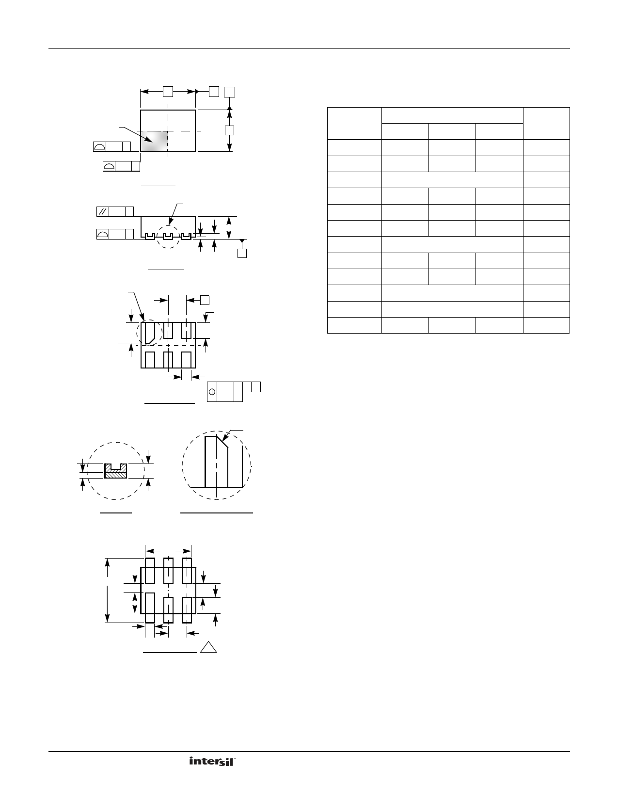
Ultra Thin Dual Flat No-Lead Plastic Package (UTDFN)
E AB
PIN 1
REFERENCE
2X 0.10 C
2X 0.10 C
TOP VIEW
D
0.10 C
7X 0.08 C
DETAIL A
A
A1 A3
SIDE VIEW
C
SEATING
PLANE
DETAIL B
1
L1
4X
e
5X
3L
64
BOTTOM VIEW
b 6X
0.10 C A B
0.05 C NOTE 3
0.1x45°
CHAMFER
A1 A3
DETAIL A
DETAIL B PIN 1 LEAD
L6.1.2x1.0A
6 LEAD ULTRA THIN DUAL FLAT NO-LEAD PLASTIC PACKAGE
MILLIMETERS
SYMBOL
MIN NOMINAL MAX
NOTES
A
0.45 0.50 0.55
-
A1 - - 0.05 -
A3 0.127 REF -
b
0.15 0.20 0.25
5
D
0.95 1.00 1.05
-
E
1.15 1.20 1.25
-
e
0.40 BSC
-
L
0.30 0.35 0.40
-
L1 0.40 0.45 0.50 -
N 62
Ne 3 3
0 - 12 4
NOTES:
Rev. 2 8/06
1. Dimensioning and tolerancing conform to ASME Y14.5-1994.
2. N is the number of terminals.
3. Ne refers to the number of terminals on E side.
4. All dimensions are in millimeters. Angles are in degrees.
5. Dimension b applies to the metallized terminal and is measured
between 0.15mm and 0.30mm from the terminal tip.
6. The configuration of the pin #1 identifier is optional, but must be
located within the zone indicated. The pin #1 identifier may be
either a mold or mark feature.
7. Maximum package warpage is 0.05mm.
8. Maximum allowable burrs is 0.076mm in all directions.
9. JEDEC Reference MO-255.
10. For additional information, to assist with the PCB Land Pattern
Design effort, see Intersil Technical Brief TB389.
1.00
1.40
0.20
0.45
0.30
0.35
0.20
0.40
LAND PATTERN 10
11 FN6552.2
October 23, 2009
11 Page | ||
| Páginas | Total 12 Páginas | |
| PDF Descargar | [ Datasheet ISL54504.PDF ] | |
Hoja de datos destacado
| Número de pieza | Descripción | Fabricantes |
| ISL54500 | Single SPDT Analog Switch | Intersil Corporation |
| ISL54501 | Single SPST Analog Switches | Intersil |
| ISL54502 | Single SPST Analog Switches | Intersil |
| ISL54504 | Single SPST Analog Switches | Intersil |
| Número de pieza | Descripción | Fabricantes |
| SLA6805M | High Voltage 3 phase Motor Driver IC. |
Sanken |
| SDC1742 | 12- and 14-Bit Hybrid Synchro / Resolver-to-Digital Converters. |
Analog Devices |
|
DataSheet.es es una pagina web que funciona como un repositorio de manuales o hoja de datos de muchos de los productos más populares, |
| DataSheet.es | 2020 | Privacy Policy | Contacto | Buscar |
