|
|
|
PDF ISL78843ASRH Data sheet ( Hoja de datos )
| Número de pieza | ISL78843ASRH | |
| Descripción | High Performance Industry Standard Single-Ended Current Mode PWM Controller | |
| Fabricantes | Intersil | |
| Logotipo | ||
Hay una vista previa y un enlace de descarga de ISL78843ASRH (archivo pdf) en la parte inferior de esta página. Total 16 Páginas | ||
|
No Preview Available !
DATASHEET
Radiation Hardened, High Performance Industry
Standard Single-Ended Current Mode PWM Controller
ISL78840ASEH, ISL78841ASEH, ISL78843ASEH, ISL78845ASEH
ISL78840ASRH, ISL78841ASRH, ISL78843ASRH, ISL78845ASRH
The ISL78840ASEH, ISL78841ASEH, ISL78843ASEH,
ISL78845ASEH, ISL78840ASRH, ISL78841ASRH,
ISL78843ASRH, ISL78845ASRH are a high performance,
radiation hardened drop-in replacement for the popular 28C4x
and 18C4x PWM controllers suitable for a wide range of power
conversion applications including boost, flyback and isolated
output configurations. Its fast signal propagation and output
switching characteristics make this an ideal product for
existing and new designs.
Features include up to 13.2V operation, low operating current,
90µA typical start-up current, adjustable operating frequency
to 1MHz and high peak current drive capability with 50ns rise
and fall times.
Features
• Electrically screened to DLA SMD #5962-07249
• QML Qualified Per MIL-PRF-38535 Requirements
• 1A MOSFET Gate Driver
• 90µA typical start-up current, 125µA Maximum
• 35ns propagation delay current sense to output
• Fast transient response with peak current mode control
• 9V to 13.2V operation
• Adjustable switching frequency to 1MHz
• 50ns rise and fall times with 1nF output load
Applications
• Current mode switching power supplies
• Isolated buck and flyback regulators
• Boost regulators
• Trimmed timing capacitor discharge current for accurate
deadtime/maximum duty cycle control
• 1.5MHz bandwidth error amplifier
• Tight tolerance voltage reference over line, load and
temperature
• Direction and speed control in motors
• ±3% current limit threshold
• Control of high current FET drivers
• Pb-free available (RoHS compliant)
Related Literature
• TR005, “Single Event Effects (SEE) Test Report for
ISL78843ASRH and ISL78845ASRH High Performance
Single-ended Current Mode PWM Controllers”
• TR006, “Neutron Testing of the ISL78845ASEH Pulse Width
Modulator”
• Radiation environment:
- High dose rate (50 - 300rad(Si)/s). . . . . . . . . . 100krad(Si)
- Low dose rate (0.01rad(Si)/s) . . . . . . . . . . . . 100krad(Si)*
* Product capability established by initial characterization. The
“EH” version is acceptance tested on a wafer by wafer basis to
50krad(Si) at low dose rate. (Applies for ISL7884xASEH only)
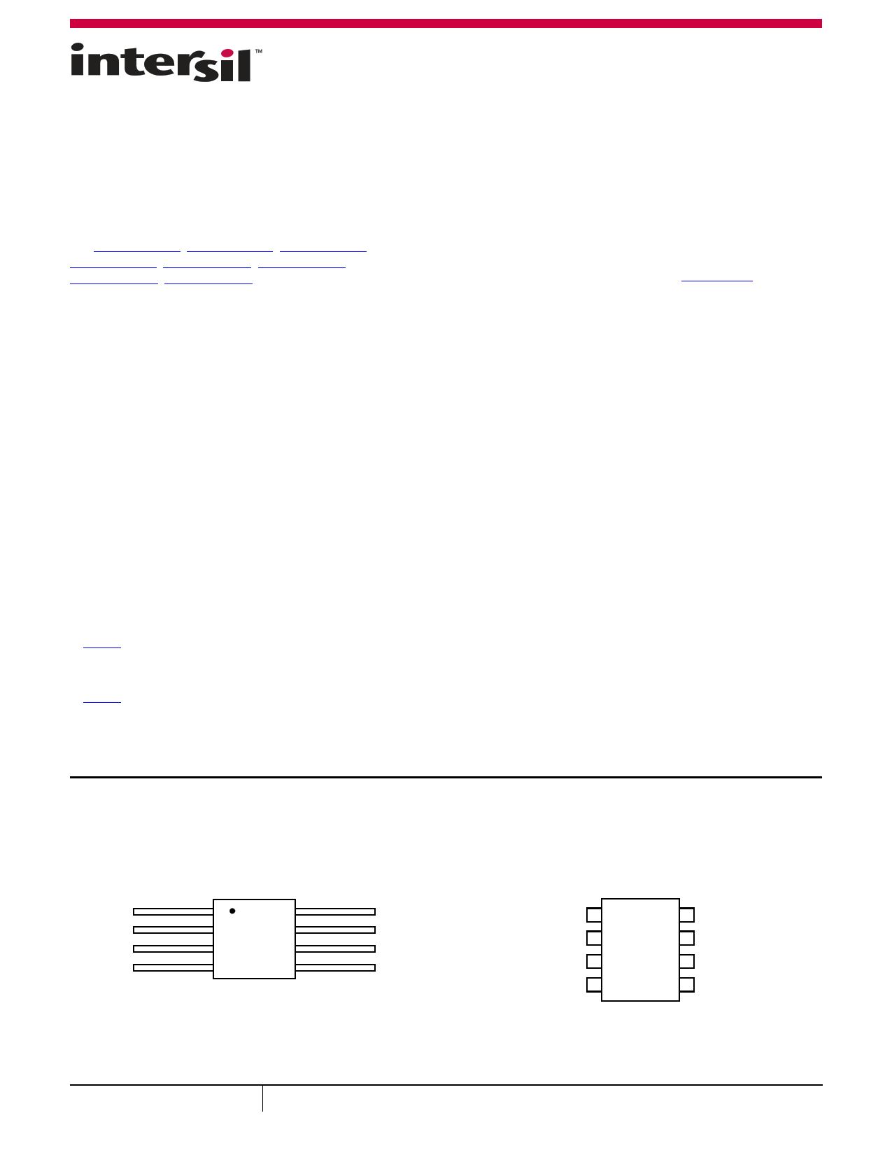
Pin Configurations
ISL78840ASEH, ISL78841ASEH,
ISL78843ASEH, ISL78845ASEH ISL78840ASRH,
ISL78841ASRH, ISL78843ASRH, ISL78845ASRH
(8 LD FLATPACK)
TOP VIEW
COMP
FB
CS
RTCT
18
27
36
45
VREF
VDD
OUT
GND
ISL78840ASEH, ISL78841ASEH,
ISL78843ASEH, ISL78845ASEH ISL78840ASRH,
ISL78841ASRH, ISL78843ASRH, ISL78845ASRH
(8 LD SBDIP)
TOP VIEW
COMP 1
FB 2
CS 3
RTCT 4
8 VREF
7 VDD
6 OUT
5 GND
April 8, 2016
FN7952.1
1
CAUTION: These devices are sensitive to electrostatic discharge; follow proper IC Handling Procedures.
1-888-INTERSIL or 1-888-468-3774 | Copyright Intersil Americas LLC 2012, 2016. All Rights Reserved
Intersil (and design) is a trademark owned by Intersil Corporation or one of its subsidiaries.
All other trademarks mentioned are the property of their respective owners.
1 page 
Functional Block Diagram
VDD
GND
START/STOP
UV COMPARATOR
+ VDD OK
-
+-
2.5V
A
A = 0.5
VREF
5V
ENABLE
VREF FAULT -
+
VREF
UV COMPARATOR
4.65V 4.80V
PWM
COMPARATOR
CS +
100mV
-
FB
COMP
+
-
ERROR
AMPLIFIER
2R
VF TOTAL = 1.15V R
1.1V
CLAMP
VREF
100k
150k
RTCT
2.9V
1.0V
ON
OSCILLATOR
COMPARATOR
<10ns
-
+ CLOCK
8.4mA
ON
ONLY
ISL78841A,
ISL78845A
Q
T
Q
SQ
RQ
RESET
DOMINANT
FIGURE 1. BLOCK DIAGRAM
36k
VREF
OUT
5 Page 
ISL78840ASEH, ISL78841ASEH, ISL78843ASEH, ISL78845ASEH ISL78840ASRH, ISL78841ASRH, ISL78843ASRH, ISL78845ASRH
The COMP pin is clamped to the voltage on capacitor C1 plus a
base-emitter junction by transistor Q1. C1 is charged from VREF
through resistor R1 and the base current of Q1. At power-up C1 is
fully discharged, COMP is at ~0.7V and the duty cycle is zero. As
C1 charges, the voltage on COMP increases and the duty cycle
increases in proportion to the voltage on C1. When COMP
reaches the steady state operating point, the control loop takes
over and soft-start is complete. C1 continues to charge up to
VREF and no longer affects COMP. During power-down, diode D1
quickly discharges C1 so that the soft-start circuit is properly
initialized prior to the next power-on sequence.
Gate Drive
The ISL7884xAxEH is capable of sourcing and sinking 1A peak
current. To limit the peak current through the IC, an optional
external resistor may be placed between the totem-pole output of
the IC (OUT pin) and the gate of the MOSFET. This small series
resistor also damps any oscillations caused by the resonant tank
of the parasitic inductances in the traces of the board and the
FETs input capacitance. TID environment of >50krads requires
the use of a bleeder resistor of 10k from the OUT pin to GND.
Slope Compensation
For applications where the maximum duty cycle is less than 50%,
slope compensation may be used to improve noise immunity,
particularly at lighter loads. The amount of slope compensation
required for noise immunity is determined empirically, but is
generally about 10% of the full scale current feedback signal. For
applications where the duty cycle is greater than 50%, slope
compensation is required to prevent instability.
Slope compensation may be accomplished by summing an
external ramp with the current feedback signal or by subtracting
the external ramp from the voltage feedback error signal. Adding
the external ramp to the current feedback signal is the more
popular method.
From the small signal current-mode model [1] it can be shown
that the naturally-sampled modulator gain, Fm, without slope
compensation is calculated in Equation 6:
Fm = S-----n---1-t--s---w---
(EQ. 6)
Where Sn is the slope of the sawtooth signal and tsw is the
duration of the half-cycle. When an external ramp is added, the
modulator gain becomes Equation 7:
Fm = ---S----n-----+-----S1-----e------t--s---w--- = m------c---S---1-n----t--s----w--
(EQ. 7)
Where Se is slope of the external ramp and becomes Equation 8:
mc = 1 + SS-----en--
(EQ. 8)
The criteria for determining the correct amount of external ramp
can be determined by appropriately setting the damping factor of
the double-pole located at the switching frequency. The
double-pole will be critically damped if the Q-factor is set to 1,
over-damped for Q < 1 and under-damped for Q > 1. An
under-damped condition may result in current loop instability.
Q = -------m-----c-----1-----–--1---D--------–-----0---.--5----
(EQ. 9)
Where D is the percent of on-time during a switching cycle.
Setting Q = 1 and solving for Se yields Equation 10:
Se
=
Sn
1--
+
0.5
1-----–-1----D---
–
1
(EQ. 10)
Since Sn and Se are the on-time slopes of the current ramp and
the external ramp, respectively, they can be multiplied by tON to
obtain the voltage change that occurs during tON.
Ve
=
Vn
1--
+
0.5
1-----–-1----D---
–
1
(EQ. 11)
Where Vn is the change in the current feedback signal (I) during
the on-time and Ve is the voltage that must be added by the
external ramp.
For a flyback converter, Vn can be solved in terms of input
voltage, current transducer components and primary inductance,
yielding Equation 12:
Ve
=
D---------T----S----W-------L---Vp----I--N--------R-----C----S--
1--
+
0.5
1-----–-1----D---
–
1
V
(EQ. 12)
Where RCS is the current sense resistor, Tsw is the switching
period, Lp is the primary inductance, VIN is the minimum input
voltage and D is the maximum duty cycle.
The current sense signal at the end of the ON time for CCM
operation is Equation 13:
VCS = N-----S----N----RP-----C----S-- IO + ---1-----–----D-------2----L-V--s--O--------T----s---w--
V
(EQ. 13)
Where VCS is the voltage across the current sense resistor, Ls is
the secondary winding inductance and IO is the output current at
current limit. Equation 13 assumes the voltage drop across the
output rectifier is negligible.
Since the peak current limit threshold is 1.00V, the total current
feedback signal plus the external ramp voltage must sum to this
value when the output load is at the current limit threshold as
shown in Equation 14:
Ve + VCS = 1V
(EQ. 14)
Substituting Equations 12 and 13 into Equation 14 and solving
for RCS yields Equation 15:
RCS = -D-----------------T--------s--L----w----p--------------V--------I----N--------------1------1------+----–-----0----D---.---5------–---1--------+---1--N-N--------p-s-----------I--O-----+-----------1---------–---------D-------------2--------L--V-----s---O-----------------T--------s------w-------
(EQ. 15)
Submit Document Feedback 11
FN7952.1
April 8, 2016
11 Page | ||
| Páginas | Total 16 Páginas | |
| PDF Descargar | [ Datasheet ISL78843ASRH.PDF ] | |
Hoja de datos destacado
| Número de pieza | Descripción | Fabricantes |
| ISL78843ASRH | High Performance Industry Standard Single-Ended Current Mode PWM Controller | Intersil |
| Número de pieza | Descripción | Fabricantes |
| SLA6805M | High Voltage 3 phase Motor Driver IC. |
Sanken |
| SDC1742 | 12- and 14-Bit Hybrid Synchro / Resolver-to-Digital Converters. |
Analog Devices |
|
DataSheet.es es una pagina web que funciona como un repositorio de manuales o hoja de datos de muchos de los productos más populares, |
| DataSheet.es | 2020 | Privacy Policy | Contacto | Buscar |