|
|
|
PDF ISL95712 Data sheet ( Hoja de datos )
| Número de pieza | ISL95712 | |
| Descripción | Multiphase PWM Regulator | |
| Fabricantes | Intersil | |
| Logotipo | ||
Hay una vista previa y un enlace de descarga de ISL95712 (archivo pdf) en la parte inferior de esta página. Total 30 Páginas | ||
|
No Preview Available !
DATASHEET
Multiphase PWM Regulator for AMD Fusion™ Desktop
CPUs Using SVI 2.0
ISL95712
The ISL95712 is fully compliant with AMD Fusion™ SVI 2.0 and
provides a complete solution for microprocessor and graphics
processor core power. The ISL95712 controller supports two
Voltage Regulators (VRs) for Core and Northbridge outputs. The
Core VR can be configured for 4-, 3-, 2-, or 1-phase operation while
the Northbridge VR supports 3-, 2- or 1-phase configurations for
maximum flexibility. The two VRs share a serial control bus to
communicate with the AMD CPU and achieve lower cost and
smaller board area compared with two-chip solutions.
The PWM modulator is based on Intersil’s Robust Ripple
Regulator R3™ Technology. Compared to traditional modulators,
the R3™ modulator can automatically change switching
frequency for faster transient settling time during load transients
and improved light load efficiency.
The ISL95712 has several other key features. Both outputs
support DCR current sensing with a single NTC thermistor for
DCR temperature compensation or accurate resistor current
sensing. They also utilize remote voltage sense, adjustable
switching frequency, OC protection and power-good indicators.
Applications
• AMD Fusion CPU/GPU core power
• Desktop computers
Features
• Supports AMD SVI 2.0 serial data bus interface and PMBus
- Serial VID clock frequency range 100kHz to 25MHz
• Dual output controller with 12V integrated core gate drivers
• Precision voltage regulation
- 0.5% system accuracy over-temperature
- 0.5V to 1.55V in 6.25mV steps
- Enhanced load line accuracy
• Supports multiple current sensing methods
- Lossless inductor DCR current sensing
- Precision resistor current sensing
• Programmable 1-, 2-, 3- or 4-phase for the core output and
1- , 2- or 3-phase for the Northbridge output
• Adaptive body diode conduction time reduction
• Superior noise immunity and transient response
• Output current and voltage telemetry
• Differential remote voltage sensing
• High efficiency across entire load range
• Programmable slew rate
• Programmable VID offset and droop on both outputs
• Programmable switching frequency for both outputs
• Excellent dynamic current balance between phases
• Protection: OCP/WOC, OVP, PGOOD and thermal monitor
• Small footprint 52 Ld 6x6 QFN package
- Pb-free (RoHS compliant)
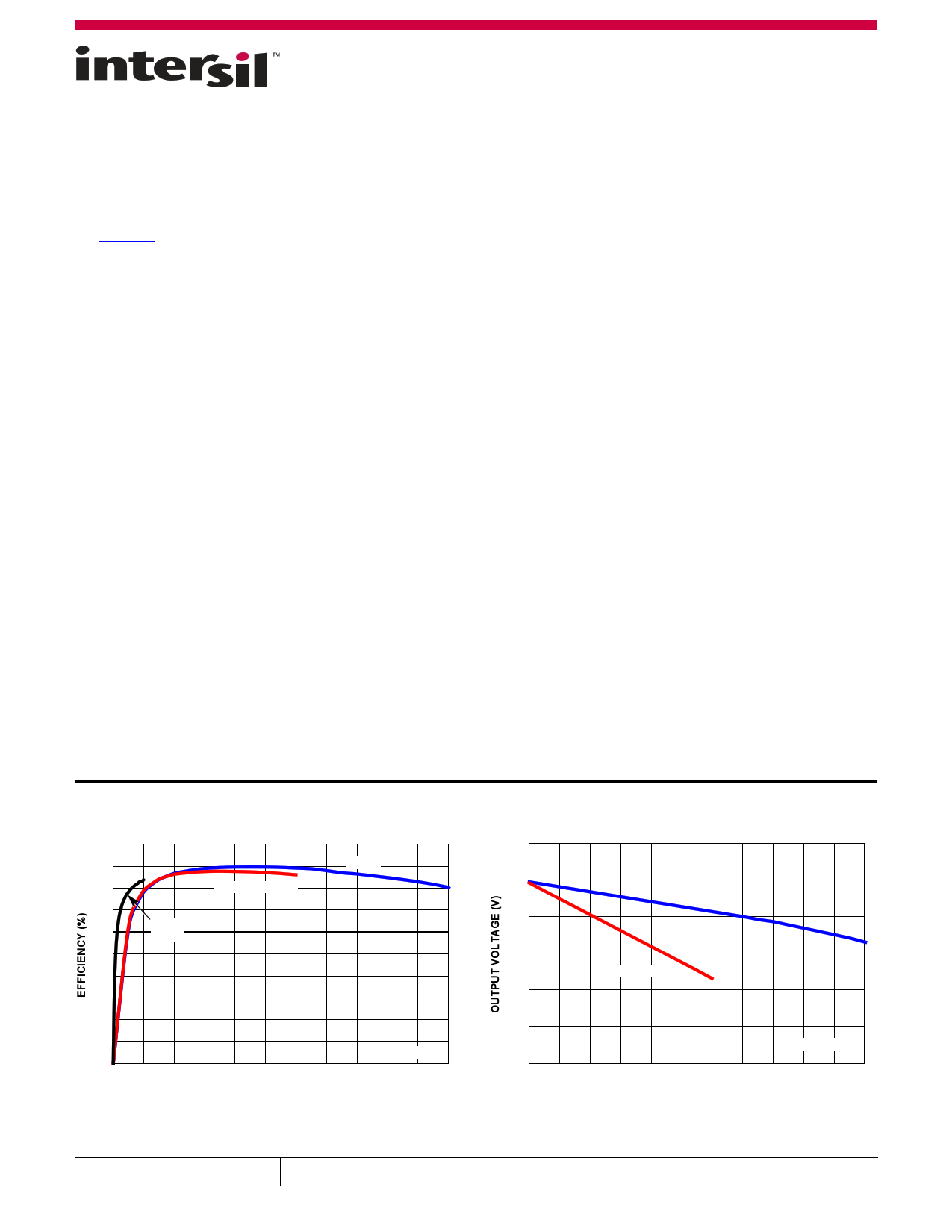
Performance
100
90
80
70
60
50
40
30
20
10
0
0
CORE
(PSI1)
NORTHBRIDGE
CORE
DAC = 1.500V
10 20 30 40 50 60 70 80 90 100 110
LOAD CURRENT (A)
FIGURE 1. EFFICIENCY vs LOAD
1.6
1.5
CORE
1.4
1.3
NORTHBRIDGE
1.2
1.1
DAC = 1.500V
1.0
0 10 20 30 40 50 60 70 80 90 100 110
LOAD CURRENT (A)
FIGURE 2. VOUT vs LOAD
November 2, 2015
FN8566.1
1
CAUTION: These devices are sensitive to electrostatic discharge; follow proper IC Handling Procedures.
1-888-INTERSIL or 1-888-468-3774 | Copyright Intersil Americas LLC 2014, 2015. All Rights Reserved
Intersil (and design) and R3 Technology are trademarks owned by Intersil Corporation or one of its subsidiaries.
All other trademarks mentioned are the property of their respective owners.
1 page 
ISL95712
Pin Descriptions (Continued)
PIN NUMBER
14
15
16
17
18
19
20
21
22
23
24
25
26
27
28
29
30
31
32
33
34
35
36
SYMBOL
ISEN3
ISEN2
ISEN1
ISUMP
ISUMN
VSEN
RTN
FB
VDD
PGOOD
COMP
BOOT1
PHASE1
UGATE1
LGATE1
BOOT2
PHASE2
UGATE2
VDDP
LGATE2
LGATE1_NB
PHASE1_NB
UGATE1_NB
DESCRIPTION
ISEN3 is the individual current sensing for Channel 3 of the Core VR. When ISEN3 is pulled to +5V, the
controller disables Channel 3, and the Core VR runs in two-phase mode.
Individual current sensing for Channel 2 of the Core VR. When ISEN2 is pulled to +5V, the controller
disables Channel 2, and the Core VR runs in single-phase mode.
Individual current sensing for Channel 1 of the Core VR. If ISEN2 is tied to +5V, this pin cannot be left
open and must be tied to GND with a 10kΩ resistor. If ISEN1 is tied to +5V, the Core portion of the IC is
shut down.
Noninverting input of the transconductance amplifier for current monitor and load line of Core output.
Inverting input of the transconductance amplifier for current monitor and load line of Core output.
Output voltage sense pin for the Core controller. Connect to the +sense pin of the microprocessor die.
Output voltage sense return pin for both Core VR and Northbridge VR. Connect to the -sense pin of the
microprocessor die.
Output voltage feedback to the inverting input of the Core controller error amplifier.
5V bias power. A resistor [2Ω] and a decoupling capacitor should be used from the +5V supply. A high
quality, X7R dielectric MLCC capacitor is recommended.
Open-drain output to indicate the Core output is ready to supply regulated voltage. Pull-up externally to
VDD or 3.3V through a resistor.
Core controller error amplifier output. A resistor from COMP to GND sets the Core VR offset voltage.
Connect an MLCC capacitor across the BOOT1 and PHASE1 pins. The boot capacitor is charged, through
an internal boot diode connected from the VDDP pin to the BOOT1 pin, each time the PHASE1 pin drops
below VDDP minus the voltage dropped across the internal boot diode.
Current return path for the Phase 1 high-side MOSFET gate driver of VR1. Connect the PHASE1 pin to the
node consisting of the high-side MOSFET source, the low-side MOSFET drain and the output inductor of
Phase 1.
Output of the Phase 1 high-side MOSFET gate driver of the Core VR. Connect the UGATE1 pin to the gate
of the Phase 1 high-side MOSFET(s).
Output of the Phase 1 low-side MOSFET gate driver of the Core VR. Connect the LGATE1 pin to the gate
of the Phase 1 low-side MOSFET(s).
Connect an MLCC capacitor across the BOOT2 and PHASE2 pins. The boot capacitor is charged, through
an internal boot diode connected from the VDDP pin to the BOOT2 pin, each time the PHASE2 pin drops
below VDDP minus the voltage dropped across the internal boot diode.
Current return path for the Phase 2 high-side MOSFET gate driver of the Core VR. Connect the PHASE2
pin to the node consisting of the high-side MOSFET source, the low-side MOSFET drain and the output
inductor of Phase 2.
Output of the Phase 2 high-side MOSFET gate driver of the Core VR. Connect the UGATE2 pin to the gate
of the Phase 2 high-side MOSFET(s).
Input voltage bias for the internal gate drivers. Connect +12V to the VDDP pin. Decouple with at least 1µF
of capacitance to GND. A high quality, X7R dielectric MLCC capacitor is recommended.
Output of the Phase 2 low-side MOSFET gate driver of the Core VR. Connect the LGATE2 pin to the gate
of the Phase 2 low-side MOSFET(s).
Output of Northbridge Phase 1 low-side MOSFET gate driver. Connect the LGATE1_NB pin to the gate of
the Northbridge VR Phase 1 low-side MOSFET(s).
Current return path for Northbridge VR Phase 1 high-side MOSFET gate driver. Connect the PHASE1_NB
pin to the node consisting of the high-side MOSFET source, the low-side MOSFET drain and the output
inductor of Northbridge Phase 1.
Output of the Phase 1 high-side MOSFET gate driver of the Northbridge VR. Connect the UGATE1_NB pin
to the gate of the Northbridge VR Phase 1 high-side MOSFET(s).
Submit Document Feedback
5
FN8566.1
November 2, 2015
5 Page 
VCRM
MASTER
CLOCK
CLOCK1
PWM1
CLOCK2
PWM2
PWM
CLOCK3
PWM3
VW
COMP
VW
ISL95712
Figure 9 shows the operation principle in diode emulation mode at
light load. The load gets incrementally lighter in each of the three
cases from top to bottom. The PWM on-time is determined by the
VW window size and therefore is the same, making the inductor
current triangle the same in each of the three cases. The ISL95712
clamps the ripple capacitor voltage VCRS in DE mode to make it
mimic the inductor current. It takes the COMP voltage longer to hit
VCRS, naturally stretching the switching period. The inductor
current triangles move farther apart, such that the inductor current
average value is equal to the load current. The reduced switching
frequency helps increase light-load efficiency.
VCRS
CCM/DCM BOUNDARY
VW
IL
VCRS
VW LIGHT DCM
VCRS1
VCRS3
VCRS2
FIGURE 7. R3™ MODULATOR OPERATION PRINCIPLES IN LOAD
INSERTION RESPONSE
Diode Emulation and Period Stretching
The ISL95712 can operate in Diode Emulation (DE) mode to
improve light-load efficiency. In DE mode, the low-side MOSFET
conducts when the current is flowing from source-to-drain and
does not allow reverse current, thus emulating a diode. Figure 8
shows when LGATE is on, the low-side MOSFET carries current,
creating negative voltage on the phase node due to the voltage
drop across the ON-resistance. The ISL95712 monitors the current
by monitoring the phase node voltage. It turns off LGATE when the
phase node voltage reaches zero to prevent the inductor current
from reversing the direction and creating unnecessary power loss.
PHASE
UGATE
LGATE
IL
FIGURE 8. DIODE EMULATION
If the load current is light enough, as Figure 8 shows, the inductor
current reaches and stays at zero before the next phase node
pulse, and the regulator is in Discontinuous Conduction Mode
(DCM). If the load current is heavy enough, the inductor current
will never reach 0A, and the regulator is in CCM, although the
controller is in DE mode.
IL
VCRS
DEEP DCM
VW
IL
FIGURE 9. PERIOD STRETCHING
Channel Configuration
Individual PWM channels of either VR can be disabled by
connecting the ISENx pin of the channel not required to +5V. For
example, placing the controller in a 3+1 configuration, requires
ISEN4 of the Core VR and ISEN2_NB and ISEN3_NB of the
Northbridge VR to be tied to +5V. This disables Channel 4 of the
Core VR and Channels 2 and 3 of the Northbridge VR. ISEN1_NB
must be tied through a 10kΩ resistor to GND to prevent this pin
from pulling high and disabling the channel. Similarly, if the Core
VR is set to single phase mode, ISEN4, ISEN3 and ISEN2 will be
tied to +5V while ISEN1 is tied to GND through a 10kΩ resistor.
Connecting ISEN1 or ISEN1_NB to +5V will disable the
corresponding VR output. This feature allows debugging of
individual VR outputs.
Power-On Reset
Before the controller has sufficient bias to guarantee proper
operation, the ISL95712 requires a +5V input supply tied to VDD
to exceed the VDD rising Power-On Reset (POR) threshold. Once
this threshold is reached or exceeded, the ISL95712 has enough
bias to check the state of the SVI inputs once ENABLE is taken
high. Hysteresis between the rising and the falling thresholds
assure the ISL95712 does not inadvertently turn off unless the
bias voltage drops substantially (see “Electrical Specifications”
on page 7). Note that VIN must be present for the controller to
drive the output voltage.
Submit Document Feedback 11
FN8566.1
November 2, 2015
11 Page | ||
| Páginas | Total 30 Páginas | |
| PDF Descargar | [ Datasheet ISL95712.PDF ] | |
Hoja de datos destacado
| Número de pieza | Descripción | Fabricantes |
| ISL95710 | 128 Taps Up/Down Interface | Intersil Corporation |
| ISL95711 | 128 Taps I2C Serial Interface | Intersil Corporation |
| ISL95712 | Multiphase PWM Regulator | Intersil |
| Número de pieza | Descripción | Fabricantes |
| SLA6805M | High Voltage 3 phase Motor Driver IC. |
Sanken |
| SDC1742 | 12- and 14-Bit Hybrid Synchro / Resolver-to-Digital Converters. |
Analog Devices |
|
DataSheet.es es una pagina web que funciona como un repositorio de manuales o hoja de datos de muchos de los productos más populares, |
| DataSheet.es | 2020 | Privacy Policy | Contacto | Buscar |