|
|
|
PDF SP3220EU Data sheet ( Hoja de datos )
| Número de pieza | SP3220EU | |
| Descripción | +3.0V to +5.5V RS-232 Driver/Receiver Pair | |
| Fabricantes | Exar | |
| Logotipo | ||
Hay una vista previa y un enlace de descarga de SP3220EU (archivo pdf) en la parte inferior de esta página. Total 19 Páginas | ||
|
No Preview Available !
SP3220E/EB/EU
+3.0V to +5.5V RS-232 Driver/Receiver Pair
FEATURES
■ Meets all EIA/TIA-232-F Standards
from a +3.0V to +5.5V power supply
• Interoperable with RS-232 and V.28 at +2.7V
■ Supports High Serial Data Rates:
• 120kbps SP3220E
• 250kbps SP3220EB
• 1Mbps SP3220EU
■ 1µA Low Power Shutdown Mode
■ Footprint Compatible with MAX3221E, ISL3221
■ 4 x 1.0µF External Charge Pump Capacitors
■ Improved ESD Specifications:
+15kV Human Body Model
+15kV IEC61000-4-2 Air Discharge
+8kV IEC61000-4-2 Contact Discharge
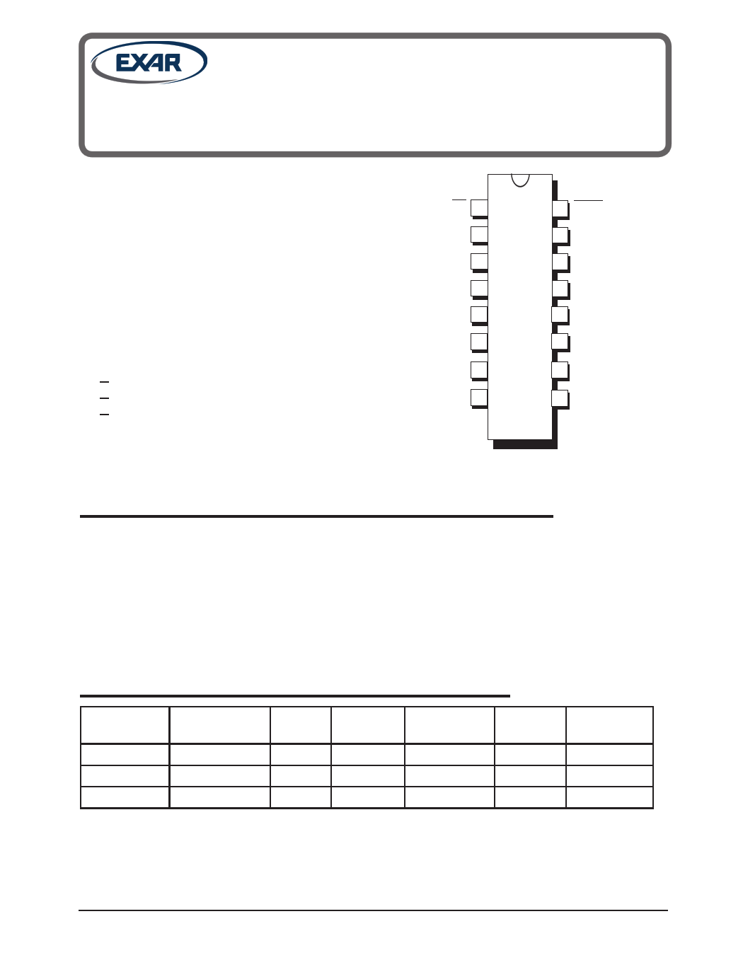
EN 1
C1+ 2
V+ 3
C1- 4
C2+ 5
C2- 6
V- 7
R1IN 8
16 SHDN
15 VCC
14 GND
SP3220 13 T1OUT
E/EB/EU
12 No Connect
11 T1IN
10 No Connect
9 R1OUT
Now Available in Lead Free Packaging
DESCRIPTION
The SP3220E devices are RS-232 driver/receiver solutions intended for portable or hand-held
applications such as palmtop computers, instrumentation and consumer products. These
devices incorporate a high-efficiency, charge-pump power supply that allows the SP3220E
devices to deliver true RS-232 performance from a single power supply ranging from +3.0V
to +5.0V. This charge pump requires only 0.1µF capacitors in 3.3V operation. The ESD toler-
ance of the these devices are over +/-15kV for both Human Body Model and IEC61000-4-2
Air discharge test methods. All devices have a low-power shutdown mode where the driver
outputs and charge pumps are disabled. During shutdown, the supply current falls to less
than 1µA.
SELECTION TABLE
MODEL
SP3220E
SP3220EB
SP3220EU
Power
Supplies
+3.0V to +5.5V
+3.0V to +5.5V
+3.0V to +5.5V
RS-232
Drivers
1
1
1
RS-232
Receivers
1
1
1
External
Components
4 Capacitors
4 Capacitors
4 Capacitors
Shutdown
Yes
Yes
Yes
Data Rate
120kbps
250kbps
1Mbps
Exar Corporation 48720 Kato Road, Fremont CA, 94538 • 510-668-7017 • www.exar.com
1
SP3220E_EB_EU_102_102016
1 page 
TYPICAL PERFORMANCE CHARACTERISTICS: Continued
Unless otherwise noted, the following performance characteristics apply for VCC = +3.3V, 250kbps data rate, all
drivers loaded with 3kΩ, 0.1µF charge pump capacitors, and TAMB = +25°C.
6
4
2
0
-2
-4
-6 0
2Mbps
1.5Mbps
1Mbps
2Mbps
1.5Mbps
1Mbps
250
500
1000
Load Capacitance (pF)
1500
2000
Figure 7. Transmitter Output Voltage vs Load
Capacitance for the SP3220EU.
6
4
2
0
-2
-4
-6
2.5
2.7
TxOUT+
TxOUT-
3 3.5 4
Supply V oltage (V)
4.5 5
Figure 8. Transmitter Output Voltage vs Supply
Voltage for the SP3220EU.
16
14
12
10
8
6
4
T1 Loaded with 3K // 1000pf @1Mbps
2
0
2.7 3 3.5 4
Supply Voltage (V)
4.5
5
Figure 9. Supply Current vs Supply Voltage for the
SP3220EU.
Exar Corporation 48720 Kato Road, Fremont CA, 94538 • 510-668-7017 • www.exar.com
5
SP3220E_EB_EU_102_102016
5 Page 
Charge Pump
The charge pump is an Exar-patended
design (U.S. 5,306,954) and uses a unique
approach compared to older less-efficient
designs. The charge pump still requires four
external capacitors, but uses a four-phase
voltage shifting technique to attain sym-
metrical 5.5V power supplies. The internal
power supply consists of a regulated dual
charge pump that provides output voltages
of +/-5.5V regardless of the input voltage
(Vcc) over the +3.0V to +5.5V range.
In most circumstances, decoupling the
power supply can be achieved adequately
using a 0.1µF bypass capacitor at C5 (refer
to figures 6 and 7). In applications that are
sensitive to power-supply noise, decouple
Vcc to ground with a capacitor of the same
value as charge-pump capacitor C1. Physi-
cally connect bypass capacitor as close to
the IC as possible.
The charge pump operates in a discontinu-
ous mode using an internal oscillator. If the
output voltages are less than a magnitude
of 5.5V, the charge pump is enabled. If the
output voltages exceed a magnitude of 5.5V,
the charge pump is disabled. This oscillator
controls the four phases of the voltage shift-
ing. A description of each phase follows.
Phase 1
—of thVeSScclohcakrgcyecsleto, rthaegepo—sitDivuersinidgethoifscpahpaascei-
tCinnoelr+Ccsits1eC–tdih1seattornnadVsnwCsCCfi,et2crtahhrereeeddvittnoooilttCGiaa2gNl–le.yDSpcaiohnntacedrengttCehiade2l+ctaioshcacrVoroCgsnCes-.
capacitor C2 is now 2 times VCC.
Phase 2
— VSS transfer — Phase two of the clock
connects the negative terminal of C2 to the VSS
storage capacitor and the positive terminal of
Cat2etdovGoNltaDg.eTthoisCt3r.aTnhsisfegrsenaenreagteadtivveolgtaegneeirs-
regulated to a minimum voltage of -5.5V.
DESCRIPTION
Simultaneous with the transfer of the volt-
age to C3, the positive side of capacitor C1
is switched to VCC and the negative side is
connected to GND.
Phase 3
— VDD charge storage — The third phase of
the clock is identical to the first phase — the
cthheanrgeegatrtaivnestfeerrmreidnainl oCf C1 1p,rwodhuiccheiss a–pVpCClieidn
tCiso22+thisteimanteeVsgCaVCt,CivCth.eesvidoeltaogfecappoatecnittoiarlCa2c.roSsisncCe2
Phase 4
— VDD transfer — The fourth phase of
the clock connects the negative terminal
of C2 to GND, and transfers this positive
gVeDDnesratoteradgevocltaapgaeciatocrr.ossThCis2 tvooltCa4g,ethies
regulated to +5.5V. At this voltage, the in-
ternal oscillator is disabled. Simultaneous
with the
positive
transfer
side of
coafptahceitovroltCa1geistoswCit4c, htehde
to VCC and the negative side is con-
nected to GND, allowing the charge
pump cycle to begin again. The charge
pump cycle will continue as long as the
operational conditions for the internal
oscillator are present.
Since both V+ and V– are separately gener-
ated
and
from
V– will
VCC, in a no–load
be symmetrical.
condition V+
Older charge
pump approaches that generate V– from
V+ will show a decrease in the magnitude
of V– compared to V+ due to the inherent
inefficiencies in the design.
Exar Corporation 48720 Kato Road, Fremont CA, 94538 • 510-668-7017 • www.exar.com
11
SP3220E_EB_EU_102_102016
11 Page | ||
| Páginas | Total 19 Páginas | |
| PDF Descargar | [ Datasheet SP3220EU.PDF ] | |
Hoja de datos destacado
| Número de pieza | Descripción | Fabricantes |
| SP3220E | +3.0V to +5.5V RS-232 Driver/Receiver Pair | Exar |
| SP3220E | +3.0V to +5.5V RS-232 Driver/Receiver Pair | Sipex |
| SP3220EB | +3.0V to +5.5V RS-232 Driver/Receiver Pair | Exar |
| SP3220EU | +3.0V to +5.5V RS-232 Driver/Receiver Pair | Exar |
| Número de pieza | Descripción | Fabricantes |
| SLA6805M | High Voltage 3 phase Motor Driver IC. |
Sanken |
| SDC1742 | 12- and 14-Bit Hybrid Synchro / Resolver-to-Digital Converters. |
Analog Devices |
|
DataSheet.es es una pagina web que funciona como un repositorio de manuales o hoja de datos de muchos de los productos más populares, |
| DataSheet.es | 2020 | Privacy Policy | Contacto | Buscar |