|
|
|
PDF CYWB0224ABS Data sheet ( Hoja de datos )
| Número de pieza | CYWB0224ABS | |
| Descripción | USB and Mass Storage Peripheral Controller | |
| Fabricantes | Cypress Semiconductor | |
| Logotipo | ||
Hay una vista previa y un enlace de descarga de CYWB0224ABS (archivo pdf) en la parte inferior de esta página. Total 30 Páginas | ||
|
No Preview Available !
CYWB022XX Family
West Bridge®: Astoria™
USB and Mass Storage Peripheral Controller
West Bridge®: Astoria™ USB and Mass Storage Peripheral Controller
Features
■ Multimedia device support
❐ Up to two SD, SDIO, MMC, MMC+, and CE-ATA devices
■ Supports Microsoft® Media Transfer Protocol (MTP) with
optimized data throughput
■ Simultaneous Link to Independent Multimedia (SLIM®)
architecture, enabling simultaneous and independent data
paths between the processor and USB, and between the USB
and mass storage
■ High-speed USB at 480 Mbps
❐ USB 2.0 compliant
❐ Integrated USB switch
❐ Integrated USB 2.0 transceiver, smart serial interface engine
❐ 16 programmable endpoints
■ GPIF (General Programmable Interface)
❐ Allows direct connection to most parallel interface
❐ Programmable waveform descriptors and configuration
registers to define waveforms
❐ Supports multiple Ready (RDY) inputs and Control (CTL)
outputs
■ Flexible processor interface that supports:
❐ Multiplexing and nonmultiplexing address and data interface
❐ SRAM interface
❐ Pseudo cellular random access memory (CRAM) interface
(Antioch interface)
❐ Pseudo NAND flash interface
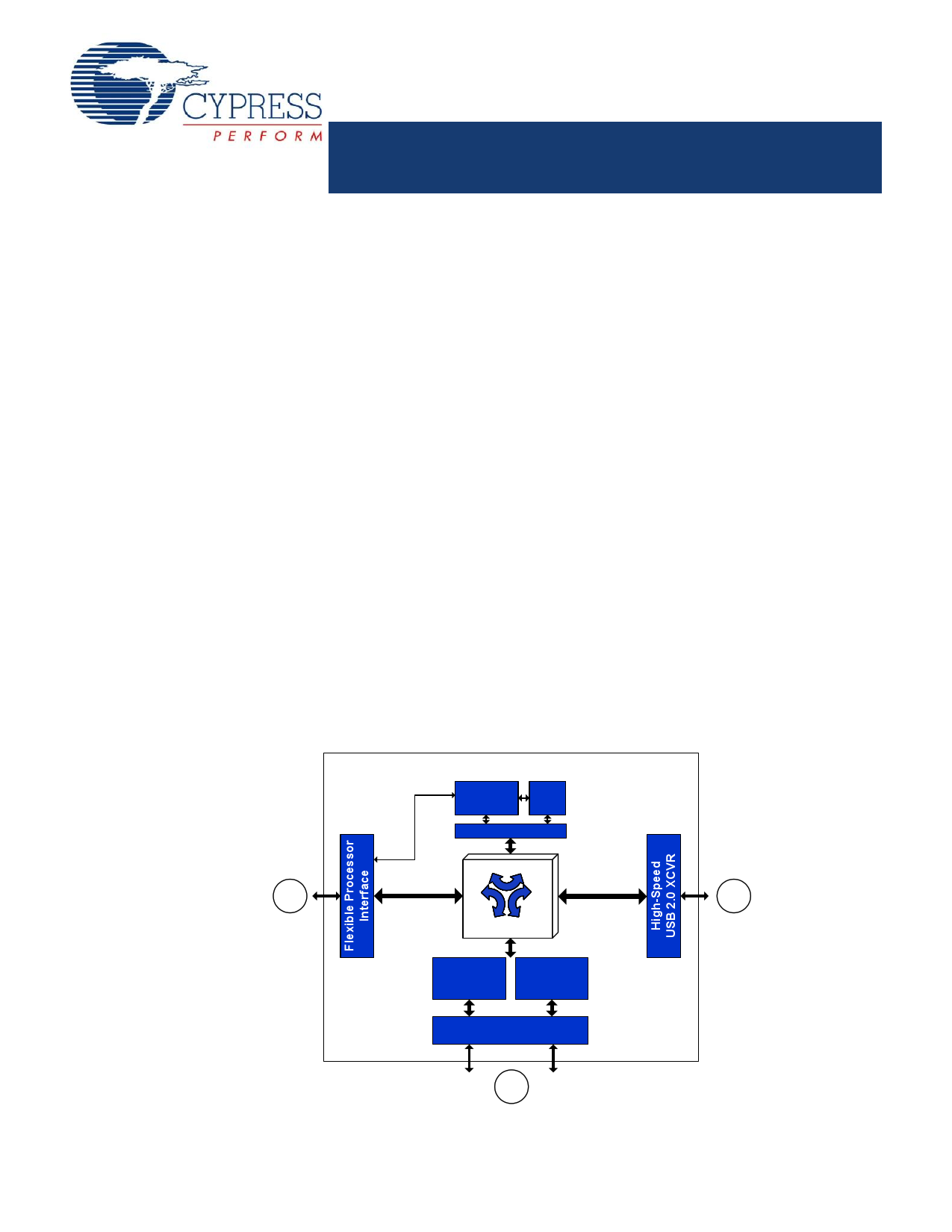
Logic Block Diagram
❐ SPI (slave mode) interface
❐ Direct memory access (DMA) slave support
■ FlexBoot
❐ Processor can boot from the processor interface port
■ Ultra low power, 1.8-V core operation
■ Low power modes
■ Small footprint:
❐ 3.91 × 3.91 × 0.55 mm 81-ball WLCSP (SP and Lite SP)
❐ 6 × 6 × 1.0 mm 100-ball VFBGA
❐ 10 × 10 × 1.20 mm 121-ball FBGA
■ Supports USB Boot, I2C Boot and Processor Boot
■ Selectable clock input frequencies
❐ 19.2 MHz, 24 MHz, 26 MHz, and 48 MHz
Applications
■ Cellular phones
■ Portable media players
■ Personal digital assistants
■ Portable navigation devices
■ Digital cameras
■ POS terminals
■ Portable video recorders
■ Data cards and wireless dongles
West BridgeTM AstoriaTM
Control
Registers
uC
Access Control
P
SLIMTM
U
SD/SDIO/
Cypress
MMC+/ CE- N-XpressTM
ATA Block Engine
Configurable Storage
Interface
S
Cypress Semiconductor Corporation • 198 Champion Court
Document Number: 001-13805 Rev. *O
• San Jose, CA 95134-1709 • 408-943-2600
Revised December 1, 2014
1 page 
CYWB022XX Family
GPIF and GPIO Interface
The GPIF and GPIO interface mode configure the S-Port to
support GPIF and GPIO as shown in Figure 5. Each GPIO is
configured as either input or output independently. The
processor accesses those GPIO through the P-Port driver’s API.
Figure 5. GPIF and GPIO Interface Mode
GPIO Interface Mode
The GPIO interface mode configures the S-Port to all GPIO as
shown in Figure 6. Each GPIO is configured as either input or
output independently. The processor accesses those GPIO
through the P-Port driver’s API.
Figure 6. GPIO Interface Mode
Astoria
S Port
GPIO
SD/SDIO/MMC+/CE-ATA Port (S-Port)
When Astoria is configured with firmware to support SD, SDIO,
MMC+, and CE-ATA, this interface supports:
■ The Multimedia Card System Specification, MMCA Technical
Committee, Version 4.1
■ SD Memory Card Specification – Part 1, Physical Layer
Specification, SD Group, Version 1.10, October 15, 2004
■ SD Memory Card Specification – Part 1, Physical Layer
Specification, SD Group, Version 2.0, May 9, 2006
■ SD Specifications – Part E1 SDIO Specification, Version 1.10,
August 18, 2004
■ CE-ATA Specification – CE-ATA Digital Protocol, CE-ATA
Committee, Version 1.1, September, 2005
West Bridge Astoria provides support for 1-bit and 4-bit SD;
SDIO cards; 1-bit, 4-bit, and 8-bit MMC; MMC+ cards; and
CE-ATA drive. For the SD, SDIO, MMC/MMC Plus, and CE-ATA,
this block supports one card for one physical bus interface.
Astoria supports SD commands including the multisector
program command that are handled by the API.
GPIO Port (S-Port)
The GPIO in S-Port is configurable as either input or output
direction independently. The processor accesses the GPIO
through the P-Port driver’s API.
Clocking
Astoria allows connection of a crystal between the XTALIN and
XTALOUT pins or an external clock at the XTALIN pin. The
81-ball WLCSP package only supports the external clock. The
power supply level at the crystal supply XVDDQ determines
whether a crystal or a clock is provided. If XVDDQ is detected to
be 1.8 V, Astoria assumes that a clock input is provided. For a
crystal to be connected, XVDDQ must be 3.3 V.
Note Clock inputs at 3.3 V level are not supported.
Astoria’s 100-ball VFBGA package supports external crystal and
clock inputs at 19.2, 24, and 26 MHz frequencies. At 48 MHz,
only clock inputs are supported. The 81-ball SPWLCSP only
supports 19.2 and 26 MHz external clock input. The 81-ball Lite
SP WLCSP only supports 26 MHz external clock or crystal input.
The crystal or clock frequency selection is shown in Table 1 on
page 6, Table 2 on page 6, and Table 3 on page 6.
The XTALIN frequency is independent of the clock and data rate
of the 8051 microprocessor or any of the device interfaces
(including P-Port and S-Port). The internal PLL applies the
proper clock multiply option depending on the input frequency.
For applications that use an external clock source to drive
XTALIN, the XTALOUT pin must be left floating. The external
clock source must also stop high or low and not toggle, to
achieve the lowest possible current consumption. The
requirements for an external clock source are shown in Table 4
on page 6.
Astoria has an on-chip oscillator circuit that uses an external
19.2, 24, and 26 MHz (±150 ppm) crystal with the following
characteristics:
■ Parallel resonant
■ Fundamental mode
■ 1 mW drive level
■ 12 pF (5% tolerance) load capacitors
■ 150 ppm
Document Number: 001-13805 Rev. *O
Page 5 of 78
5 Page 
Table 6. Astoria 100-ball VFBGA Package Pin Assignments (continued)
C5 XTALSLC[1]
C4 XTALSLC[0]
E8 TEST[2]
C8 TEST[1]
D7 TEST[0]
A8 XTALIN
B8 XTALOUT
D4, PVDDQ
H4
H5 SNVDDQ
B5 UVDDQ
H7 SSVDDQ
D6 GVDDQ
B9 AVDDQ
B7 XVDDQ
D5, VDD
G4,
G5,
G6,
G7,
F7
A10 VDD33
B6 UVSSQ
A9 AVSSQ
E4, VGND
E5,
E6,
E7,
F4,
F5,
F6
Pin Name
CYWB022XX Family
Pin Description
I Clock Select 1
Clock Select 0
I Test Cfg 2
Test Cfg 1
Test Cfg 0
I Crystal/Clock IN
O Crystal Out
Power Processor I/F VDD
Power
Domain
GVDDQ
VGND
XVDDQ
VGND
Power GPIF VDD
Power USB VDD
Power SDIO VDD
Power Misc I/O VDD
Power Analog VDD
Power Crystal VDD
Power Core VDD
Power Independent 3.3 V
Power USB GND
Power Analog GND
Power Core GND
Document Number: 001-13805 Rev. *O
Page 11 of 78
11 Page | ||
| Páginas | Total 30 Páginas | |
| PDF Descargar | [ Datasheet CYWB0224ABS.PDF ] | |
Hoja de datos destacado
| Número de pieza | Descripción | Fabricantes |
| CYWB0224ABM | USB and Mass Storage Peripheral Controller | Cypress Semiconductor |
| CYWB0224ABM | West Bridge Astoria | Cypress Semiconductor |
| CYWB0224ABS | USB and Mass Storage Peripheral Controller | Cypress Semiconductor |
| CYWB0224ABS | West Bridge Astoria | Cypress Semiconductor |
| Número de pieza | Descripción | Fabricantes |
| SLA6805M | High Voltage 3 phase Motor Driver IC. |
Sanken |
| SDC1742 | 12- and 14-Bit Hybrid Synchro / Resolver-to-Digital Converters. |
Analog Devices |
|
DataSheet.es es una pagina web que funciona como un repositorio de manuales o hoja de datos de muchos de los productos más populares, |
| DataSheet.es | 2020 | Privacy Policy | Contacto | Buscar |