|
|
|
PDF AD9554 Data sheet ( Hoja de datos )
| Número de pieza | AD9554 | |
| Descripción | Multiservice Line Card Adaptive Clock Translator | |
| Fabricantes | Analog Devices | |
| Logotipo | ||
Hay una vista previa y un enlace de descarga de AD9554 (archivo pdf) en la parte inferior de esta página. Total 30 Páginas | ||
|
No Preview Available !
Data Sheet
Quad PLL, Quad Input, Multiservice Line
Card Adaptive Clock Translator
AD9554
FEATURES
Supports GR-1244 Stratum 3 stability in holdover mode
Supports smooth reference switchover with virtually no
disturbance on output phase
Supports Telcordia GR-253 jitter generation, transfer, and
tolerance for SONET/SDH up to OC-192 systems
Supports ITU-T G.8262 synchronous Ethernet slave clocks
Supports ITU-T G.823, ITU-T G.824, ITU-T G.825, and
ITU-T G.8261
Auto/manual holdover and reference switchover
Adaptive clocking allows dynamic adjustment of feedback
dividers for use in OTN mapping/demapping applications
Quad digital phase-locked loop (DPLL) architecture with four
reference inputs (single-ended or differential)
4 × 4 crosspoint allows any reference input to drive any PLL
Input reference frequencies from 2 kHz to 1000 MHz
Reference validation and frequency monitoring: 2 ppm
Programmable input reference switchover priority
20-bit programmable input reference divider
8 differential clock outputs with each differential pair
configurable as HCSL, LVDS-compatible, or LVPECL-
compatible
Output frequency range: 430 kHz to 941 MHz
Programmable 18-bit integer and 24-bit fractional feedback
divider in digital PLL
Programmable loop bandwidths from 0.1 Hz to 4 kHz
Optional off-chip EEPROM to store power-up profile
72-lead (10 mm × 10 mm) LFCSP package
APPLICATIONS
Network synchronization, including synchronous Ethernet
and synchronous digital hierarchy (SDH) to optical
transport network (OTN) mapping/demapping
Cleanup of reference clock jitter
SONET/SDH clocks up to OC-192, including FEC
Stratum 3 holdover, jitter cleanup, and phase transient
control
Cable infrastructure
Data communications
Professional video
GENERAL DESCRIPTION
The AD9554 is a low loop bandwidth clock translator that
provides jitter cleanup and synchronization for many systems,
including synchronous optical networks (SONET/SDH). The
AD9554 generates an output clock synchronized to up to four
external input references. The digital PLL (DPLL) allows for
reduction of input time jitter or phase noise associated with the
external references. The digitally controlled loop and holdover
circuitry of the AD9554 continuously generates a low jitter
output clock even when all reference inputs have failed.
The AD9554 operates over an industrial temperature range of
−40°C to +85°C. If a smaller device is needed, the AD9554-1 is
a version of this device with one output per PLL. If a single or
dual DPLL version of this device is needed, refer to the AD9557
or AD9559, respectively.
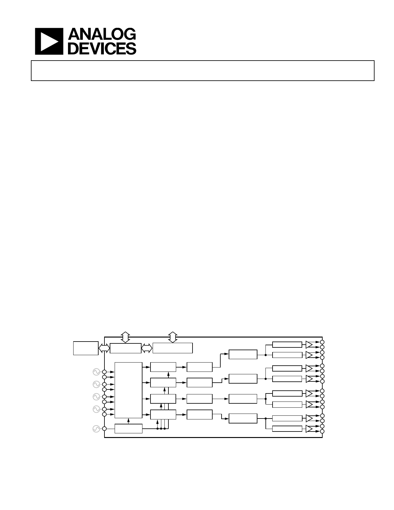
FUNCTIONAL BLOCK DIAGRAM
EXTERNAL
EEPROM
(OPTIONAL)
STABLE
SOURCE
STATUS AND
CONTROL PINS
REFERENCE
INPUT
MONITOR
AND MUX
CLOCK
MULTIPLIER
SERIAL INTERFACE
(SPI OR I2C)
DIGITAL
PLL 0
DIGITAL
PLL 1
ANALOG
PLL 0
ANALOG
PLL 1
P0 DIVIDER
P1 DIVIDER
DIGITAL
PLL 2
DIGITAL
PLL 3
ANALOG
PLL 2
ANALOG
PLL 3
P2 DIVIDER
P3 DIVIDER
AD9554
Figure 1.
Q0_A DIVIDER
Q0_B DIVIDER
Q1_A DIVIDER
Q1_B DIVIDER
Q2_A DIVIDER
Q2_B DIVIDER
Q3_A DIVIDER
Q3_B DIVIDER
Rev. C
Document Feedback
Information furnished by Analog Devices is believed to be accurate and reliable. However, no
responsibilityisassumedbyAnalogDevices for itsuse,nor foranyinfringementsofpatentsor other
rights of third parties that may result from its use. Specifications subject to change without notice. No
license is granted by implication or otherwise under any patent or patent rights of Analog Devices.
Trademarksandregisteredtrademarksarethepropertyoftheirrespectiveowners.
One Technology Way, P.O. Box 9106, Norwood, MA 02062-9106, U.S.A.
Tel: 781.329.4700 ©2014–2016 Analog Devices, Inc. All rights reserved.
Technical Support
www.analog.com
1 page 
AD9554
REVISION HISTORY
10/2016—Rev. B to Rev. C
Changes to Multifunction Pins at Reset/Power-Up Section
and Table 21..................................................................................... 25
Changes to Figure 29...................................................................... 29
Changes to the Important Update to EEPROM Programing
Sequence Section ............................................................................ 48
Changes to Table 71 and Table 73 ................................................ 82
6/2016—Rev. A to Rev. B
Changes to Device Register Programming Using a Register
Setup File Section ........................................................................... 25
Added Figure 26 to Figure 29; Renumbered Sequentially ........ 26
Added Note 1, Table 69.................................................................. 81
Changes to Bit 1 Description, Table 98........................................ 90
8/2014—Rev. 0 to Rev. A
Changes to Applications and General Description Sections ...... 1
Added Output Frequency of 0.430 MHz (Min) and
941 MHz (Max); Table 8 ................................................................ 10
Added Bandwidth (fREF = 19.44 MHz; fOUT = 156.25 MHz;
fLOOP = 50 Hz) Parameters; Table 18 ............................................. 15
Changes to Figure 3........................................................................ 21
Changes to Figure 24 Caption....................................................... 24
Changes to Table 21 and Device Register Programming Using a
Register Setup File Section ............................................................ 25
Changes to Overview Section ....................................................... 30
Data Sheet
Changes to DPLL Overview Section and Figure 27 .................. 32
Changes to System Clock (SYSCLK) Section ............................. 35
Changes to APLL Calibration Section......................................... 37
Changes to P Dividers and Output Amplitude and
Power-Down Sections.................................................................... 38
Changes to EEPROM Overview Section and Figure 32............ 41
Changes to Second Paragraph of Serial Port Control Section.. 45
Changes to Write Section, Address Ascension Section and
Table 25 ............................................................................................ 46
Changes to Data Transfer Process Section.................................. 48
Changes to Write Detect Registers Section................................. 51
Changes to Table 32 ....................................................................... 54
Changes to Table 47 ....................................................................... 71
Changes to Table 61 and Table 62 ................................................ 74
Changes to Table 68 ....................................................................... 76
Changes to Table 71 ....................................................................... 78
Changes to Table 76 ....................................................................... 79
Changes to Table 78 and Table 79 ................................................ 80
Changes to Table 100 ..................................................................... 87
Changes to Table 118 ..................................................................... 94
Changes to Table 121 ..................................................................... 96
Changes to Table 126 ..................................................................... 99
Changes to Table 155 ................................................................... 110
4/2014—Revision 0: Initial Version
Rev. C | Page 4 of 116
5 Page 
AD9554
Parameter
Duty Cycle
Up to fOUT = 750 MHz
Up to fOUT = 941 MHz
Up to fOUT = 1250 MHz
Differential Output Voltage Swing
Min
45
44
No External Termination Resistor
With 50 Ω Termination Resistor to Ground
on Each Leg
Common-Mode Output Voltage
779
413
206
Reference Input-to-Output Delay Variation
over Temperature
Static Phase Offset Variation from Active
Reference to Output over Voltage
Extremes
28 mA (LVPECL-COMPATIBLE) MODE
Output Frequency
0.430
Continuous Output Frequency Range
Maximum Output Frequency
PLL0 to PLL3 Using Unique VCO
Frequencies
PLL0, PLL1, and PLL2
PLL3
Rise/Fall Time (20% to 80%)1
Duty Cycle
Up to fOUT = 750 MHz
Up to fOUT = 941 MHz
Up to fOUT = 1250 MHz
Differential Output Voltage Swing
0.430
45
44
540
Common-Mode Output Voltage
Reference Input-to-Output Delay Variation
over Temperature
Static Phase Offset Variation from Active
Reference to Output over Voltage
Extremes
275
Data Sheet
Typ Max
50 55
50 56
50
1180
625
312
600
±75
1510
800
400
Unit Test Conditions/Comments
%
%
%
mV
mV
mV
fs/°C
fs/mV
Differential voltage swing between output pins;
measured with output driver static; peak-to-peak
differential output amplitude 2× this level with
driver toggling; see Figure 13 for output
amplitude vs. output frequency
Output driver static with 50 Ω resistor to ground
on each leg
DPLL locked to same input reference at all times;
stable system clock source (noncrystal)
941
1250
1187
185
50
50
50
830
415
600
±75
941
781
280
55
56
1020
510
Specifications for dc-coupled, 50 Ω termination
resistor from each leg to ground; ac coupling
used in most applications; output current setting
= 28 mA; in this mode, user must have either a
50 Ω resistor from each leg to ground, or a 100 Ω
resistor across the differential pair
MHz Frequency range all four PLLs can be generated
using unique VCO frequencies; frequencies
outside this range are possible on some of the PLLs,
but can result in increased VCO coupling due to
multiple PLLs using the same VCO frequency
MHz Frequency range for each PLL such that all four
PLLs are using unique VCO frequencies with no
frequency gaps
MHz Maximum frequency all four PLLs can generate
using unique VCO frequencies
MHz Limited by 1250 MHz maximum input frequency
to channel divider (Q divider)
MHz Limited by 4748 MHz maximum VCO frequency
ps
%
%
%
mV
mV
fs/°C
fs/mV
Differential voltage swing between output pins;
measured with output driver static; peak-to-peak
differential output amplitude 2× this level with
driver toggling; see Figure 10 for output
amplitude vs. output frequency
Output driver static; 50 Ω external termination
resistor from each leg to ground
DPLL locked to same input reference at all times;
stable system clock source (noncrystal)
Rev. C | Page 10 of 116
11 Page | ||
| Páginas | Total 30 Páginas | |
| PDF Descargar | [ Datasheet AD9554.PDF ] | |
Hoja de datos destacado
| Número de pieza | Descripción | Fabricantes |
| AD9550 | Integer-N Clock Translator | Analog Devices |
| AD9551 | Multiservice Clock Generator | Analog Devices |
| AD9552 | Oscillator Frequency Up Converter | Analog Devices |
| AD9553 | Flexible Clock Translator | Analog Devices |
| Número de pieza | Descripción | Fabricantes |
| SLA6805M | High Voltage 3 phase Motor Driver IC. |
Sanken |
| SDC1742 | 12- and 14-Bit Hybrid Synchro / Resolver-to-Digital Converters. |
Analog Devices |
|
DataSheet.es es una pagina web que funciona como un repositorio de manuales o hoja de datos de muchos de los productos más populares, |
| DataSheet.es | 2020 | Privacy Policy | Contacto | Buscar |