|
|
|
PDF UPD7520 Data sheet ( Hoja de datos )
| Número de pieza | UPD7520 | |
| Descripción | 4-BIT SINGLE CHIP MICROCOMPUTER | |
| Fabricantes | NEC | |
| Logotipo | ||
Hay una vista previa y un enlace de descarga de UPD7520 (archivo pdf) en la parte inferior de esta página. Total 10 Páginas | ||
|
No Preview Available !
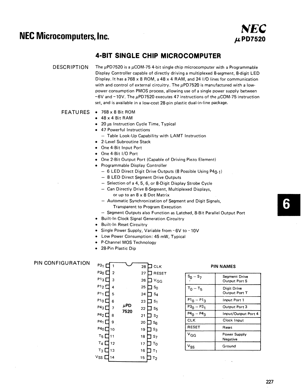
NEe Microcomputers, Inc.
NEe
,.,.PD7520
4-BIT SINGLE CHIP MICROCOMPUTER
DESCR IPTION
The j.lPD7520 is a IlCOM-75 4-bit single chip microcomputer with a Programmable
Display Controller capable of directly driving a multiplexed 8-segment, 8-digit LED
Display. It has a 768 x 8 ROM, a 48 x 4 RAM, and 24 I/O lines for communication
with and control of external circuitry. The j.lPD7520 is manufactured with a low-
power consumption PMOS process, allowing use of a single power supply between
-6V and -10V. The j.lPD7520 executes 47 instructions of the j.lCOM-75 instruction
set, and is available in a low-cost 28-pin plastic dual-in-line package.
FEATU RES
• 768 x 8 Bit ROM
• 48 x 4 Bit RAM
• 20 j.lS Instruction Cycle Time, Typical
• 47 Powerful Instructions
- Table Look-Up Capability with LAMT Instruction
• 2-Level Subroutine Stack
• One 4-Bit Input Port
• One 4-Bit I/O Port
• One 2-Bit Output Port (Capable of Driving Piezo Element)
• Programmable Display Controller
- 6 LED Direct Digit Drive Outputs (8 Possible Using P40-1)
8 LED Direct Segment Drive Outputs
Selection of a 4, 5, 6, or 8-Digit Display Strobe Cycle
Can Directly Drive 8-Segment, Multiplexed Displays,
or up to an 8 x 8 Dot Matrix
Automatic Synchronization of Segment and Digit Signals,
Transparent to Program Execution
- Segment Outputs also Function as Latched, 8-Bit Parallel Output Port
• Built-In Clock Signal Generation Circuitry
• Built-In Reset Circuitry
• Single Power Supply, Variable from -6V to -10V
• Low Power Consumption: 45 mW, Typical
• P-Channel MOS Technology
• 28-Pin Plastic Dip
PIN CONFIGURATION
P31
P30
P13
P12
P11
P10
P43
P42
P41
P40
T5
T4
T3
VSS
ClK
RESET
VGG
So
S4
S1
S5
S2
S6
S3
S7
TO
T1
T2
PIN NAMES
So -S7
TO-T5
P10 - P13
P30 - P3 1
P40 - P43
ClK
RESET
VGG
VSS
Segment Drive
Output Port S
Digit Drive
Output Port T
Input Port 1
Output Port 3
Input/Output Port 4
Clock Input
Reset
Power Supply
Negative
Ground
II
227
1 page 
J.LPD7520
Clock and Reset Circuitry
The Clock Circuitry for the J.1PD7520 can be implemented by connecting a resistor
from the ClK input to VGG. The Power-On-Reset Circuitry for the J.1PD7520 can be
implemented by connecting a capacitor from the RESET input to VSS.
I/O Capability
The J.1PD7520 has 24 I/O lines for communication with and control of external cir-
cuitry_ The Port configuration is selectable under software control via the Mode
Select Register as follows:
Port 1
Port 2
P1O-3
P2O-1
Port 3
Port 4
Port S
Port T
P3O-1
P4O-3
SO-7
TO-5
T6-7
4-Bit Schmidt Input
2-Bit latched Output Option, Accessible through
Port T (T4-5)
2-B it latched Output
4-B it Input/latched Output
latched 8-Bit Parallel/Segment Drive Output
6-Bit High-Current/Digit Drive Output
Additional 2-Bit Digit Drive Output Option, Accessible
through Port 4 (P40-1)
DISPLAY CONTROLLER
BLOCK DIAGRAM
So-7 TO-S
(TO-3. P20_11
231
5 Page | ||
| Páginas | Total 10 Páginas | |
| PDF Descargar | [ Datasheet UPD7520.PDF ] | |
Hoja de datos destacado
| Número de pieza | Descripción | Fabricantes |
| UPD7520 | 4-BIT SINGLE CHIP MICROCOMPUTER | NEC |
| UPD75206 | 4-BIT SINGLE-CHIP MICROCOMPUTER | NEC |
| UPD75208 | 4-BIT SINGLE-CHIP MICROCOMPUTER | NEC |
| UPD75212A | 4-BIT SINGLE-CHIP MICROCOMPUTER | NEC |
| Número de pieza | Descripción | Fabricantes |
| SLA6805M | High Voltage 3 phase Motor Driver IC. |
Sanken |
| SDC1742 | 12- and 14-Bit Hybrid Synchro / Resolver-to-Digital Converters. |
Analog Devices |
|
DataSheet.es es una pagina web que funciona como un repositorio de manuales o hoja de datos de muchos de los productos más populares, |
| DataSheet.es | 2020 | Privacy Policy | Contacto | Buscar |