|
|
|
PDF UM2681-3 Data sheet ( Hoja de datos )
| Número de pieza | UM2681-3 | |
| Descripción | Dual Asynchronous Receiver/Transmitter | |
| Fabricantes | UMC | |
| Logotipo | ||
Hay una vista previa y un enlace de descarga de UM2681-3 (archivo pdf) en la parte inferior de esta página. Total 23 Páginas | ||
|
No Preview Available !
(l)UMC
,===========Dual UM2681 SERIES
Wfi1 TArsaynnscmhirtotenro(uDsURAeRcTe)iver/
Features
• Dual full-duplex asynchronous receiver/transmitter
• Ouadruple buffered receiver data registers
• Programmable data format
5 to 8 data bits plus parity
Odd, even, no parity or force parity
1, 1.5 or 2 stop bits programmable in 1/16 bit
increments'
• Programmable baud rate for each receiver and
transmiter' selectable from:
18 fixed rates: 50 to 38.4K baud
One user defined rate derived from programmable
timer/counter
External 1x or 16x clock
• Parity, framing, and overrun error detection
• False start bit detection
• Line break detection and generation
• Programmable channel mode
Normal (full duplex)
Automatic echo
Localloopback
Remote loopback
• Multi-function programmable 16-bit counter/timer
• Multi-function 7-bit input port
- Can serve as clock or control inputs
- Change of state detection on four inputs
• Multi-function 8-bit output port
Individual bit set/reset capability
- Outputs can be programmed to be status/interrupt
signals
• Versatile interrupt system
Single interrupt output with eight maskable inter-
rupting conditions
Output port can be configured to provide a total of
up to six separate wire-OR'able interrupt outputs
• Maximum data transfer: 1X-l MB/sec, 16X-125KB/sec
• Automatic wake-up mode for multidrop applications
• Start-end break interrupt/status
• Detects break which originates in the middle of a
character
• On-chip crystal oscillator
• TTL compatible
• Single +5V power supply
General Description
The UM2681 Dual Universal Asynchronous Receiver/
Transmitter (DUART) is a single chip NMOS-LSI com-
munications device that provides two independent full-
duplex asynchronous receiver/transmitter channels in a
single package. It interfaces directly with microprocessors
and may be used in a polled or interrupt driven system.
The operating mode and data format of each channel can
be programmed independently. Additionally, each receiver
and transmitter can select its operating speed as one of
eighteen fixed baud rates, a 16X clock derived from a
programmable counter/timer, or an external 1X or 16X
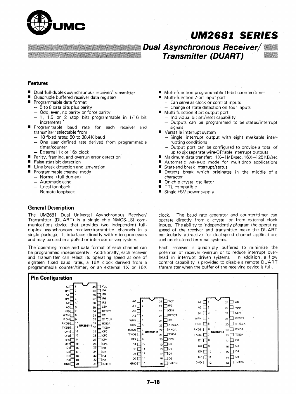
Pin Configuration
clock. The baud rate generator and counter/timer can
operate directly from a crystal or from external clock
inputs. The ability to independently program the operating
speed 'of the receiver and transmitter make the DUART
particularly attractive for dual-speed channel applications
such as clustered terminal systems.
Each receiver is quadruply buffered to minimize the
potential of receiver overrun or to reduce interrupt over-
head in interrupt driven systems. In addition, a flow
control capability is provided to disable a remote DUART
transmitter when the buffer of the receiving device is full.
OP2
OP4
OP6
DO
02
04
06
INTRN
AO
Al
A2
A3
WRN
RON
RXOB
TXOB
OPl
01
03
05
07
GNO
VCC
IP2
CEN
RESET
X2
Xl/CLK
RXOA
TXOA
OPO
DO
02
04
D6
INTRN
Al
A2
A3
WRN
RON
RXOB
TXOB
01
03
05
07
GNO
7-18
AO
Vcc
CEN
RESET
Kl/CLK
RXOA
TXOA
DO
02
04
06
INTRN
1 page 
RESET
AO-A3
CEN
RON
00-07
(READ)
WRN
00-07
(WRITE)
RON
IPO-IP6
WRN
OPO-OP7
RON
OR
WRN
INTRN
OR
OP3-0P7
UM2681 SERIES
-}---
Fi~ure 1. Reset Timing
.1
FLOAT
1__- - - - t RWO - - - -...1
Figure 2. Bus Timing
Figure 3. Port Timing
\'---"---~_tIRj_
Figure 4. Interrupt Timing
7-22
5 Page 
(IlUMC
which means one full character time of buffering is
provided. Characters cannot be loaded into the THR while
the transmitter is disabled.
The transmitter converts the parallel data from the CPU
to a serial bit stream on the TxD output pin. It
automatically sends a start bit followed by the programmed
number of data bits, an optional parity bit, and the pro-
grammed number of stop bits. The least significant bit is
sent first. Following the transmission of the stop bits, if
a new character is not available in the TH R, the TxD
output remains high and the TxEMT bit in the status
register (SR) will be set to 1. Transmission resumes and
the TxEMT bit is cleared when the CPU loads a new
character into the THR. If the transmitter is disabled, it
continues operatiRg until the character currently begin
transmitted is completely sent out. The transmitter can be
forced to send a continuous low condition by issuing a send
break command.
The transmitter can be reset through a software command.
If it is reset, operation ceases immediately and the
transmitter must be enabled through the command register
before resuming operation. If CTS operation is enabled,
the CTSN input must be low in order for the character to
be transmitted. If it goes high in the middle of a transmis-
sion, the character in the shift register is transmitted and
TxDA then remains in the marking state until CTSN goes
low. The transmi.tter can also control the deactivation of
the RTSN output. If programmed, the RTSN output will
be reset one bit time after the character in the transmit
shift register and transmit holding register (if any) are
completely transmitted, if the transmitter has been
disabled.
Receiver
The 2681 is conditioned to receive data when enabled
through the command register. The receiver looks for a
high to low (mark to space) transition of the start bit on
the RxD input pin. If a transition is detected, the state of
the RxD pin is sampled each 16X clock for 7-1/2 clocks
(16X clock mode) or at the next rising edge of the bit
time clock (1 X clock mode). ,If RxD is sampled high, the
start bit is invalid and the search for a valid start bit begins
again. If RxD is still low, a valid start bit is assumed and
the receiver continues to sample the input at one bit time
intervals at the, theoretical center of the bit, unti I the
proper number of data bits and the parity bit (if any) have
assembled, and one stop bit has been detected. The least
significant bit is received first. The data is then transferred
to the receive holding register (RHR) and the RxRDY
bit in the SR is set to a 1., This condition can be pro-
grammed to generate an interrupt at OP4 or OP5 and
INTRN. If the character legnth is less than eight bits,
the most significant unused bits in the RHR are set to
UM2681 SERIES
zero.
After the stop bit is detected, the receiver will immediately
look for the next start bit. However, if a non-zero
character was received without a stop bit (framing error)
and RxD remains low for one half of the bit period after
the stop bit was sampled, then the receiver operates as if a
new start bit transition had be'en detected at that point
(one-half bit time after the stop bit was sampled).
The parity error, framing error, overrun error and received
break state (if any)·are strobed into the SR at the received
character boundary, before the RxRDY status bit is set.
If a break condition is detected (RxD is low for the entire
character including the stop bit), a character consisting of
all zeros will be loaded into the RHR and the received
break bit in the SR is set to 1. The RxD input must return
to Cl high condition for at least one-half bit time before a
search for the next start bit begins.
The RHR consists of a first-in-first-out (FIFO) stack with
a capacity of three characters. Data is loaded from the
receive shift register into the topmost empty position of the
FIFO. The RxRDY bit in the status register is set when-
ever one or more characters are available to be read, and a
FFULL status bit is set if all three stack positions are
filled with data. Either of these bits can be selected to
cause an interrupt. A read of the R H R outputs the data at
the top of the FIFO. After the read cycle, the data FIFO
and its associated status bits (see below) are 'popped' thus
emptying a FIFO position for new data.
In addition to the data word, three status bits (parity
error, framing error, and received break) are also appended
to each data character in the FIFO (overrun is not). Status
can be provided in two ways, as programmed by the error
mode control bit in the mode register. In the 'character'
mode, status is provided on a character-by-character basis:
the status applies only to the character at the top of the
FIFO. In the 'block' mode, the status provided in the SR
for these three bits is the logical OR of the status for all
characters com ing to the top of the F I F0 si nce the last
'reset error' command was issued. In either mode reading
the SR does not affect the FIFO, The FIFO is 'popped'
only when the RHR is read. Therefore the status register
should be read prior to reading the FI FO.
If.the FIFO is full when a new character is received, that
character is held in the receive sh ift register unti I a FIFO
position is available. If an additional character is received
while this state exits, the contents of the FIFO are not
affected: the character previously in the shift register is
lost and the overrun error status bit (SR[4]) will be set
upon receipt of the start bit of the new (overruning)
character.
7-28
11 Page | ||
| Páginas | Total 23 Páginas | |
| PDF Descargar | [ Datasheet UM2681-3.PDF ] | |
Hoja de datos destacado
| Número de pieza | Descripción | Fabricantes |
| UM2681-1 | Dual Asynchronous Receiver/Transmitter | UMC |
| UM2681-2 | Dual Asynchronous Receiver/Transmitter | UMC |
| UM2681-3 | Dual Asynchronous Receiver/Transmitter | UMC |
| Número de pieza | Descripción | Fabricantes |
| SLA6805M | High Voltage 3 phase Motor Driver IC. |
Sanken |
| SDC1742 | 12- and 14-Bit Hybrid Synchro / Resolver-to-Digital Converters. |
Analog Devices |
|
DataSheet.es es una pagina web que funciona como un repositorio de manuales o hoja de datos de muchos de los productos más populares, |
| DataSheet.es | 2020 | Privacy Policy | Contacto | Buscar |