|
|
|
PDF UM9228-1 Data sheet ( Hoja de datos )
| Número de pieza | UM9228-1 | |
| Descripción | Floppy Disk Separator | |
| Fabricantes | UMC | |
| Logotipo | ||
Hay una vista previa y un enlace de descarga de UM9228-1 (archivo pdf) en la parte inferior de esta página. Total 5 Páginas | ||
|
No Preview Available !
ClUMC
:=:::::::::::: UM9228-1
Floppy Data Separator
Features
• Floppy Data Separator
Performs complete data separation function with a
little external circuit for floppy disk drives
Separates MFM encoded data
5%" double density compatible
• Early and late 250 ns write precompensation
• External 16 MHz clock required
• Compatible with the FOC 765A (8272A) floppy disk
controllers
• DMA inte"rface logic
• CMOS technology
• .Single + 5 Volt supply
• TT L compatible
• For IBM PC disk drives especially
General Description
The UM9228-1 is an CMOS integrated circuit desi~ned to
complement the 765A (8272A) type of floppy disk con-
troller chip; especially for IBM PC. It incorporates a data
separator, write precompensation logic, and DMA interface
logic. A -FDC 765A together with UM9228-1 and some
buffers qrive and decoder can be formed a IBM PC diskette
adapter. The UM9228-1 operates from a +5 Volt supply
and simply requires a 16 MHz external clock input. All
input and output are TT L compatible. The UM9228-1 is
available for 5%" double density disk controller.
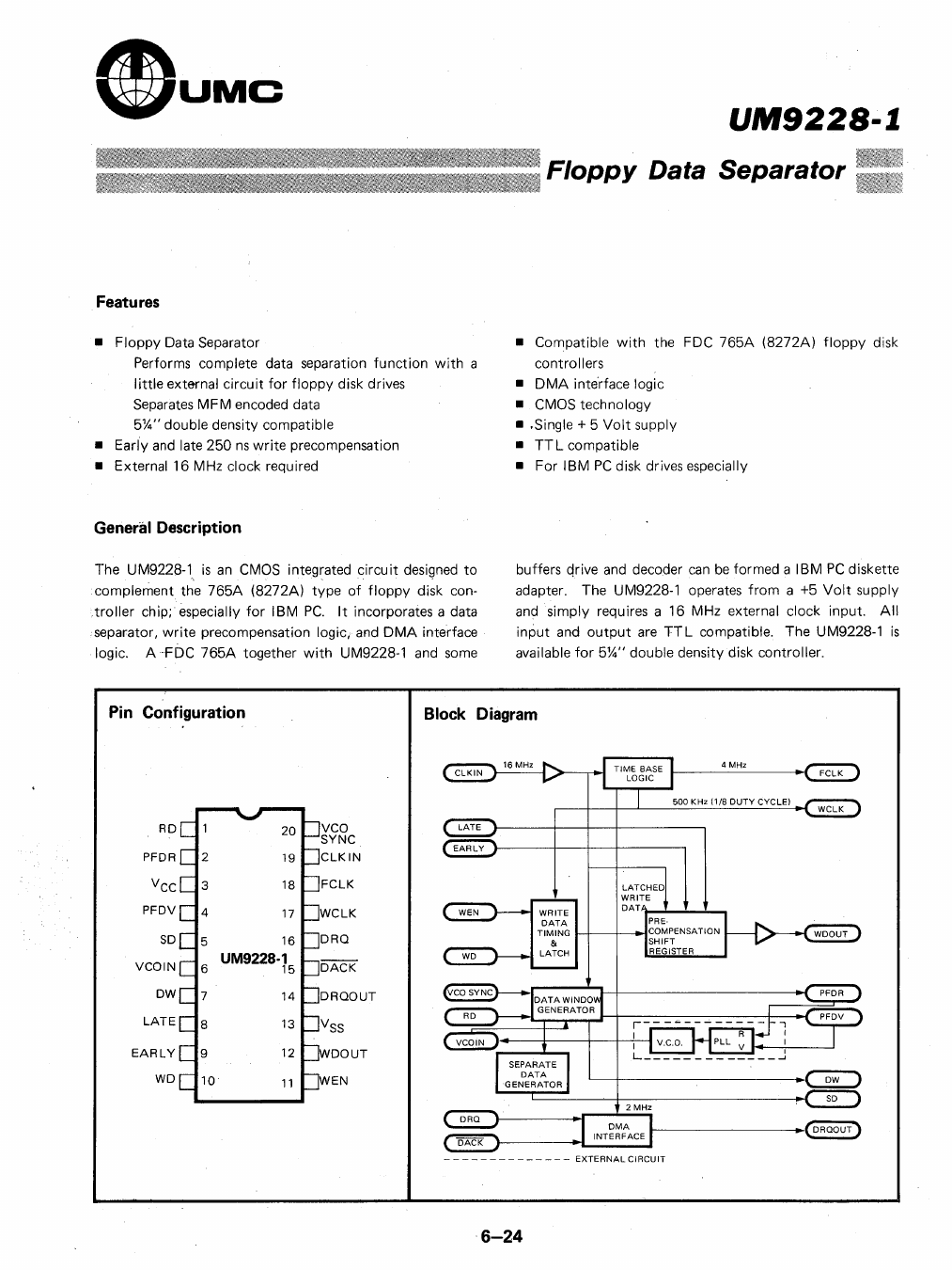
Pin Configuration
Block Diagram
RO
PFDR
Vec
PFDV
SO
VCOIN
OW
lATE
EARLY
WO
VCO
SYNC
ClKIN
FClK
ORO
OACK
OROOUT
Vss
WRITE
DATA
TIMING I-+--+-~
&
LATCH
L--r----------------_.~
~--------------_.'(DRQOUT)
)----...~.:.;,:......:.:.J
- - - - - - - - - - - - - - EXTERNAL CIRCUIT
6-24
1 page 
UM9228-1
Operational Description
DATA SEPARATOR
UM9228-1 is used with a external PLL circuit (see fig. 1) to detect the leading edges of the disk data pulse and adjust the
phase of the internal clock to provide the data window (OW) clock.
Fig. 1: Data Window Generator
The data window clock frequency is normally 250 KHz. See fig. 2.
bit cell
Data Pulse
from FDD
Data Window
MFM TYPE
Fig. 2: Data Window
TIME BASE LOGIC
It compromises 5 stages of ripple counter and a duty cycle clamping circuit. The write clock (WCLK) duty cycle is 1/S.
Ext. Clock
16MH~-------- -- - - -- -- - - - - -------llfLIUL
500KHW:...-----~===:~~~~~.,lMHW
WCLK~_ _ _ _ _ _ _ _ _ _ _ _ _ _ _ _ _ _ _ _ _ _~I
I......- - - - - - - - - - -......
- I1/8 DUTY CYCLE. 500 KHz
250ns ~
WRITE PRECOMPENSATION
The desired precompensation delay (250 ns) is determined by the state of EAR LY and LATE inputs of UM922S-1.
Nominal
Late
Early
Invalid
Early
0
0
1
1
Late
0
1
0
1
DMA INTERFACE
Fig. 3: Write Precompensation State
~
______________DRQ~________~----------------------------:----~f~~
DRQOUT,_ _ _ _ _ _ _ _ _ _ _ _ _...~. '1L...__ _ _ __
DACK
J~L...__ _ _ __
Fig. 4: DMA Interface Timing
When requiring data read/write, FOC will check OACK from OMAC and will set ORO (low to high) if OACK is high.
The DMA Interface delay ORO from FOC by 4 stage shift register as the timing shown above. This delay will prevent cpu
from being busy doing OMA without adequate system operation.
6-28
5 Page | ||
| Páginas | Total 5 Páginas | |
| PDF Descargar | [ Datasheet UM9228-1.PDF ] | |
Hoja de datos destacado
| Número de pieza | Descripción | Fabricantes |
| UM9228-1 | Floppy Disk Separator | UMC |
| Número de pieza | Descripción | Fabricantes |
| SLA6805M | High Voltage 3 phase Motor Driver IC. |
Sanken |
| SDC1742 | 12- and 14-Bit Hybrid Synchro / Resolver-to-Digital Converters. |
Analog Devices |
|
DataSheet.es es una pagina web que funciona como un repositorio de manuales o hoja de datos de muchos de los productos más populares, |
| DataSheet.es | 2020 | Privacy Policy | Contacto | Buscar |