|
|
|
PDF TOP103YAI Data sheet ( Hoja de datos )
| Número de pieza | TOP103YAI | |
| Descripción | Three-terminal Off-line PWM Switch | |
| Fabricantes | Power Integrations | |
| Logotipo | ||
Hay una vista previa y un enlace de descarga de TOP103YAI (archivo pdf) en la parte inferior de esta página. Total 20 Páginas | ||
|
No Preview Available !
TOP100-4
TOPSwitch® Family
Three-terminal Off-line PWM Switch
®
Product Highlights
Low Cost Replacement for Discrete Switchers
• 20 to 50 fewer components - cuts cost, increases reliability
• Source-connected tab and Controlled MOSFET turn-on
reduce EMI and EMI filter costs
• Allows for a 50% smaller and lighter solution
• Cost competitive with linears above 5 W
Up to 90% Efficiency in Flyback Topology
• Built-in start-up and current limit reduce DC losses
• Low capacitance 350 V MOSFET cuts AC losses
• CMOS controller/gate driver consumes only 6 mW
• 70% maximum duty cycle minimizes conduction losses
Simplifies Design - Reduces Time to Market
• Supported by many reference designs
• Integrated PWM Controller and 350 V MOSFET in a
industry standard three pin TO-220 package
• Only one external capacitor needed for compensation,
bypass and start-up/auto-restart functions
System Level Fault Protection Features
• Auto-restart and cycle by cycle current limiting functions
handle both primary and secondary faults
• On-chip latching thermal shutdown protects the entire
system against overload
Highly Versatile
• Implements Buck, Boost, Flyback or Forward topology
• Easily interfaces with both opto and primary feedback
• Supports continuous or discontinuous mode of operation
• Specified for operation down to 16 V DC input
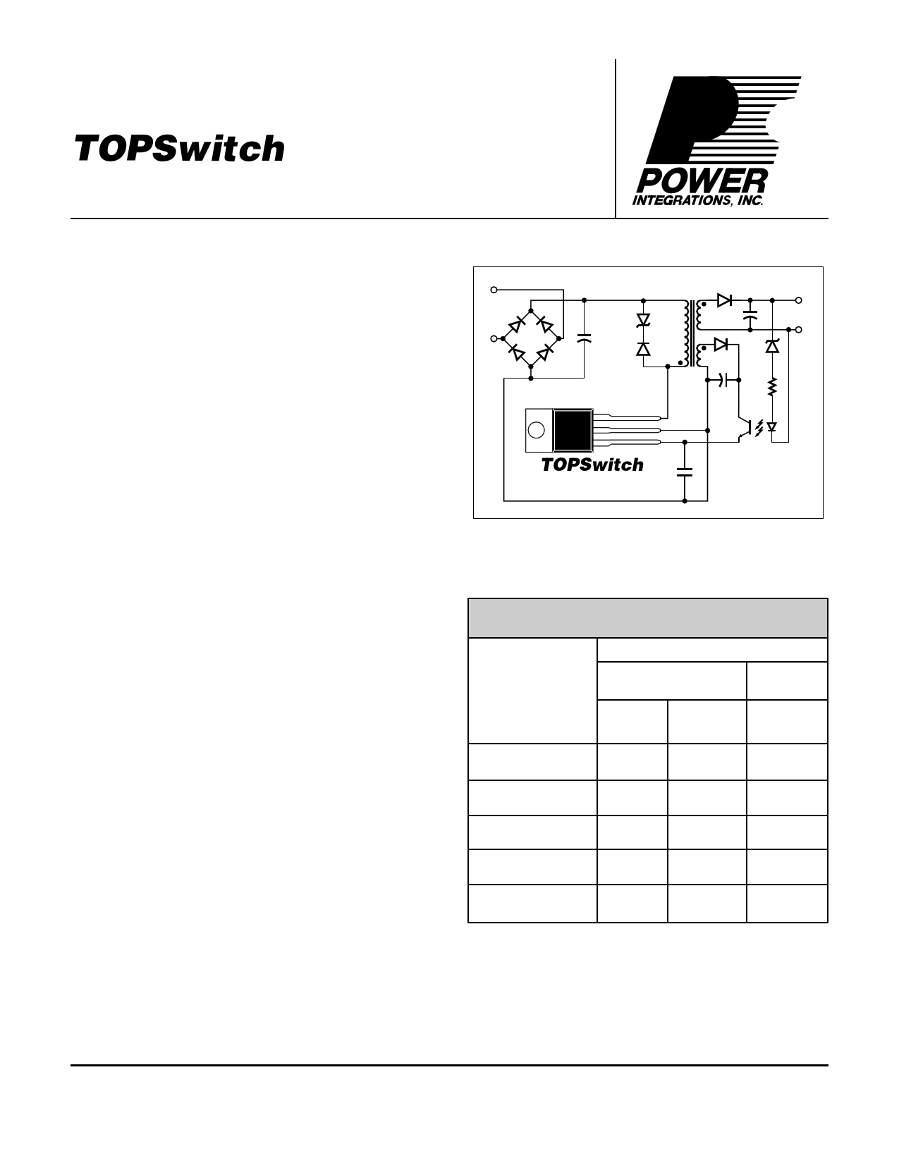
Description
The TOPSwitch family implements, with only three pins, all
functions necessary for an off-line switched mode control
system: high voltage N-channel power MOSFET with controlled
turn-on gate driver, voltage mode PWM controller with
integrated 100 kHz oscillator, high voltage start-up bias circuit,
bandgap derived reference, bias shunt regulator/error amplifier
for loop compensation and fault protection circuitry. Compared
to discrete MOSFET and controller or self oscillating (RCC)
switching converter solutions, a TOPSwitch integrated circuit
can reduce total cost, component count, size, weight and at the
same time increase efficiency and system reliability. These
AC
IN
DRAIN
SOURCE
CONTROL
TOPSwitch
Figure 1. Typical Application.
PI-1704112995
TOPSwitch SELECTION GUIDE
ORDER
PART
NUMBER
OUTPUT POWER RANGE
FLYBACK
PFC/
BOOST
100/110 V
VAC
48 V
DC
100/110
VAC
TOP100YAI* 0-20 W 0-6.8 W 0-30 W
TOP101YAI* 15-35 W 6-12 W 25-50 W
TOP102YAI* 20-45 W 8.5-17 W 35-70 W
TOP103YAI* 25-55 W 11-22 W 45-90 W
TOP104YAI* 30-60 W 12-25 W 55-110 W
* Package Outline: Y03A
devices are intended for 100/110 VAC off-line Power Supply
applications in the 0 to 60 W range and power factor correction
(PFC) applications in the 0 to 110 W range. They are also well
suited for Telecom, Cablecom and other DC to DC converter
applications in the 0-25 W range (see Design Note DN-16).
July 1996
1 page 
TOP100-4
VIN
VIN
DRAIN
0
VOUT
0
IOUT
0
VC
0
IC 0
12
812
••• •••
81
12
812
••• •••
81
45 mA
VC(reset)
1
2
34
1
PI-1119-110194
Figure 6. Typical Waveforms for (1) Normal Operation, (2) Auto-restart, (3) Latching Shutdown, and (4) Power Down Reset.
Shutdown/Auto-restart
To minimize TOPSwitch power
dissipation, the shutdown/auto-restart
circuit turns the power supply on and off
at a duty cycle of typically 5% if an out
of regulation condition persists. Loss of
regulation interrupts the external current
into the CONTROL pin. V regulation
C
changes from shunt mode to the
hysteretic auto-restart mode described
above. When the fault condition is
removed, the power supply output
becomes regulated, V regulation returns
C
to shunt mode, and normal operation of
the power supply resumes.
Latching Shutdown
The output overvoltage protection latch
is activated by a high-current pulse into
the CONTROL pin. When set, the latch
turns off the TOPSwitch output.
Activating the power-up reset circuit by
removing and restoring input power, or
momentarily pulling the CONTROL pin
below the power-up reset threshold resets
the latch and allows TOPSwitch to
resume normal power supply operation.
V is regulated in hysteretic mode when
C
the power supply is latched off.
Overtemperature Protection
Temperature protection is provided by a
precision analog circuit that turns the
output MOSFET off when the junction
temperature exceeds the thermal
shutdown temperature (typically 145°C).
Activating the power-up reset circuit by
removing and restoring input power or
momentarily pulling the CONTROL pin
below the power-up reset threshold resets
the latch and allows TOPSwitch to
resume normal power supply operation.
V is regulated in hysteretic mode when
C
the power supply is latched off.
High-voltage Bias Current Source
This current source biases TOPSwitch
from the DRAIN pin and charges the
CONTROL pin external capacitance
(C ) during start-up or hysteretic
T
operation. Hysteretic operation occurs
during auto-restart and latched
shutdown. Thecurrentsourceisswitched
on and off with an effective duty cycle of
approximately 35%. This duty cycle is
determined by the ratio of CONTROL
pin charge (I ) and discharge currents
C
(I and I ). This current source is
CD1 CD2
turned off during normal operation when
the output MOSFET is switching.
5E
7/96
5 Page 
Specification Symbol
Conditions
(Unless Otherwise Specified)
See Figure 14
SOURCE = 0 V
T
j
=
-40
to
125°C
SHUTDOWN/AUTO-RESTART (cont.)
UV Lockout
Threshold Voltage
S1 open
Auto-restart
Hysteresis Voltage
S1 open
Auto-restart
Duty Cycle
S1 open
Auto-restart
Frequency
S1 open
CIRCUIT PROTECTION
Self-protection
Current Limit
I
LIMIT
Leading Edge
Blanking Time
tLEB
TOP100
di/dt
=
160
mA/µs,
T
j
=
25˚C
TOP101
di/dt
=
280
mA/µs,
T
j
=
25˚C
TOP102
di/dt
=
400
mA/µs,
T
j
=
25˚C
TOP103
di/dt = 520 mA/µs, Tj = 25˚C
TOP104
di/dt = 600 mA/µs, Tj = 25˚C
I = 4 mA
C
Current Limit
Delay
t
ILD
I = 4 mA
C
Thermal Shutdown
Temperature
IC = 4 mA
Latched Shutdown
Trigger Current
I
SD
See Figure 13
Power-up Reset
Threshold Voltage
V
C(RESET)
S2 open
TOP100-4
Min Typ Max Units
4.7
0.6 1.0
5
1.2
8
V
V
%
Hz
0.88 1.25
1.50 2.15
2.20 3.10
2.85 4.00
3.30 4.60
150
100
125 145
25 45 75
2.0 3.3 4.2
A
ns
ns
°C
mA
V
11E
7/96
11 Page | ||
| Páginas | Total 20 Páginas | |
| PDF Descargar | [ Datasheet TOP103YAI.PDF ] | |
Hoja de datos destacado
| Número de pieza | Descripción | Fabricantes |
| TOP103YAI | Three-terminal Off-line PWM Switch | Power Integrations |
| Número de pieza | Descripción | Fabricantes |
| SLA6805M | High Voltage 3 phase Motor Driver IC. |
Sanken |
| SDC1742 | 12- and 14-Bit Hybrid Synchro / Resolver-to-Digital Converters. |
Analog Devices |
|
DataSheet.es es una pagina web que funciona como un repositorio de manuales o hoja de datos de muchos de los productos más populares, |
| DataSheet.es | 2020 | Privacy Policy | Contacto | Buscar |