|
|
PDF AD8326 Data sheet ( Hoja de datos )
| Número de pieza | AD8326 | |
| Descripción | High Output Power Programmable CATV Line Driver | |
| Fabricantes | Analog Devices | |
| Logotipo |  |
|
Hay una vista previa y un enlace de descarga de AD8326 (archivo pdf) en la parte inferior de esta página. Total 24 Páginas | ||
|
No Preview Available !
a
High Output Power
Programmable CATV Line Driver
AD8326
FEATURES
Supports DOCSIS Standard for Reverse Path
Transmission
Gain Programmable in 0.75 dB Steps over a 53.5 dB Range
Low Distortion at 65 dBmV Output
–62 dBc SFDR at 21 MHz
–58 dBc SFDR at 65 MHz
1 dB Compression of 25 dBm at 10 MHz
Output Noise Level
–45 dBmV in 160 kHz
Maintains 75 ⍀ Output Impedance
Power-Up and Power-Down Condition
Upper Bandwidth: 100 MHz (Full Gain Range)
Single or Dual Supply Operation
APPLICATIONS
Gain-Programmable Line Driver
CATV Telephony Modems
CATV Terminal Devices
General-Purpose Digitally Controlled Variable Gain Block
GENERAL DESCRIPTION
The AD8326 is a high-output power, digitally controlled, vari-
able gain amplifier optimized for coaxial line driving applications
such as data and telephony cable modems that are designed to
the MCNS-DOCSIS upstream standard. An 8-bit serial word
determines the desired output gain over a 53.5 dB range result-
ing in gain changes of 0.75 dB/LSB. The AD8326 is offered in
two models, each optimized to support the desired output power
and resulting performance.
The AD8326 comprises a digitally controlled variable attenuator
of 0 dB to –54 dB, that is preceded by a low noise, fixed-gain
buffer and is followed by a low distortion high-power amplifier.
The AD8326 accepts a differential or single-ended input signal.
The output is designed to drive a 75 Ω load, such as coaxial
cable, although the AD8326 is capable of driving other loads.
When driving 67 dBm into a 75 Ω load, the AD8326ARP
provides a worst harmonic of only –59 dBc at 21 MHz and
–57 dBc at 42 MHz. When driving 65 dBmV into a 75 Ω load,
the AD8326ARE provides a worst harmonic of only –62 dBc at
21 MHz and –60 dBc at 42 MHz.
FUNCTIONAL BLOCK DIAGRAM
VCC (7 PINS)
BYP
AD8326
VIN+
VIN–
DIFF OR
SINGLE
INPUT
AMP
VERNIER
ZIN (SINGLE) = 800⍀
ZIN (DIFF) = 1.6k⍀
ATTENUATION
CORE
8
DECODE
POWER
AMP
ZOUT DIFF =
75⍀
VOUT+
VOUT–
8
DATA LATCH
POWER-DOWN
LOGIC
8
SHIFT
REGISTER
GND
DATEN DATA CLK VEE (10 PINS) TXEN SLEEP
–40
ARP(VS = +12V)
ARE(VS = ؎5V)
–45
–50
ARP(VO = 69dBmV)
–55
ARP(VO = 67dBmV)
–60
–65 ARE(VO = 65dBmV)
–70
ARE(VO = 62dBmV)
–75
–80
5
15 25 35 45 55 65
FREQUENCY – MHz
Figure 1. Worst Harmonic Distortion vs. Frequency
The differential output of the AD8326 is compliant with DOCSIS
paragraph 4.2.10.2 for “Spurious Emissions During Burst On/Off
Transients.” In addition, this device has a sleep mode function
that reduces the quiescent current to 4 mA.
The AD8326 is packaged in a low-cost 28-lead TSSOP and a
28-lead P (power) SOIC. Both devices have an operational tem-
perature range of –40°C to +85°C.
REV. 0
Information furnished by Analog Devices is believed to be accurate and
reliable. However, no responsibility is assumed by Analog Devices for its
use, nor for any infringements of patents or other rights of third parties that
may result from its use. No license is granted by implication or otherwise
under any patent or patent rights of Analog Devices.
One Technology Way, P.O. Box 9106, Norwood, MA 02062-9106, U.S.A.
Tel: 781/329-4700
www.analog.com
Fax: 781/326-8703
© Analog Devices, Inc., 2001
1 page 
ABSOLUTE MAXIMUM RATINGS*
Supply Voltage VCC
Pins 5, 9, 10, 19, 20, 23, 27 . For ARP, Max VCC = VEE + 13 V;
. . . . . . . . . . . . . . . . . . . . . . . For ARE, Max VCC = VEE + 11 V
Input Voltages
Pins 25, 26 . . . . . . . . . . . . . . . . . . . . . . . . . . . . . . . . ± 0.5 V
Pins 1, 2, 3, 6, 7 . . . . . . . . . . . . . . . . . . . . . –0.8 V to +5.5 V
Internal Power Dissipation
TSSOP EPAD . . . . . . . . . . . . . . . . . . . . . . . . . . . . . . 1.5 W
PSOP . . . . . . . . . . . . . . . . . . . . . . . . . . . . . . . . . . . . . . 2.0 W
Operating Temperature Range . . . . . . . . . . . –40°C to +85°C
Storage Temperature Range . . . . . . . . . . . . –65°C to +150°C
Lead Temperature, Soldering 60 seconds . . . . . . . . . . . 300°C
*Stresses above those listed under Absolute Maximum Ratings may cause perma-
nent damage to the device. This is a stress rating only; functional operation of the
device at these or any other conditions above those indicated in the operational
section of this specification is not implied. Exposure to absolute maximum rating
conditions for extended periods may affect device reliability.
AD8326
Model
Temperature Range
AD8326ARP
AD8326ARP-REEL
AD8326ARP-EVAL
AD8326ARE
AD8326ARE-REEL
AD8326ARE-EVAL
–40°C to +85°C
–40°C to +85°C
*Thermal Resistance measured on SEMI standard 4-layer board.
ORDERING GUIDE
Package Description
28-Lead Power SOIC with Slug
Evaluation Board
28-Lead TSSOP with Exposed Pad
Evaluation Board
JA
23°C/W*
Package Option
RP-28
39°C/W* RE-28
CAUTION
ESD (electrostatic discharge) sensitive device. Electrostatic charges as high as 4000 V readily
accumulate on the human body and test equipment and can discharge without detection. Although
the AD8326 features proprietary ESD protection circuitry, permanent damage may occur on
devices subjected to high-energy electrostatic discharges. Therefore, proper ESD precautions are
recommended to avoid performance degradation or loss of functionality.
WARNING!
ESD SENSITIVE DEVICE
REV. 0
–5–
5 Page 
VEE
10F
VCC
DATEN
SDATA
CLK
TXEN
SLEEP
10F
0.1F
0.1F
0.1F
0.1F
0.1F
AD8326
1 DATEN
GND 28
2 SDATA
3 CLK
4 GND1
5 VCC
6 TXEN
7 SLEEP
8 GND
VCC
VIN–
VIN+
VEE
VCC
VEE
BYP
27
26
25
24
23
22
21
9 VCC
10
11
12
VCC
VEE
GND
20
VCC 19
VCC 18
VEE 17
GND
13
14
VEE
VOUT–
16
VEE 15
VOUT+
AD8326
0.1F
0.1F
0.1F
0.1F
0.1F
0.1F
0.1F
0.1F
0.1F
0.1F
165⍀
VIN–
ZIN = 150⍀
0.1F
VIN+
TOKO 617DB-A0070
TO DIPLEXER
ZIN = 75⍀
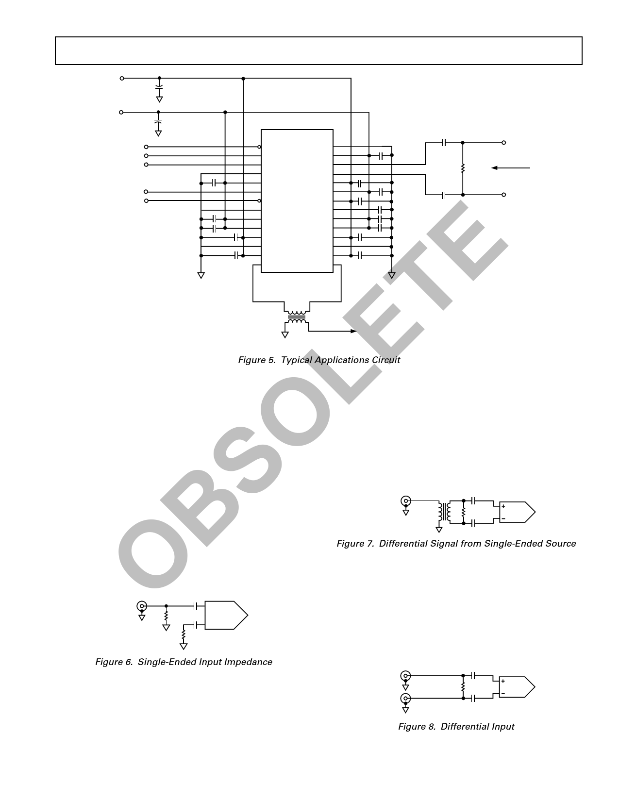
Figure 5. Typical Applications Circuit
Input Bias, Impedance, and Termination
The VIN+ and VIN– inputs have a dc bias level of approxi-
mately 1.47 V below VCC/2, therefore the input signal should
be ac-coupled using 0.1 µF capacitors as seen in the typical
application circuit (see Figure 5).
The differential input impedance of the AD8326 is approxi-
mately 1600 Ω, while the single-ended input is 800 Ω.
Single-Ended Inverting Input
When operating the AD8326 in a single-ended input mode VIN+
and VIN– should be terminated as illustrated in Figure 6. On the
AD8326 evaluation boards, this termination method requires the
removal of R12, R13, R14, R16, R17, and R18. Install a 0 Ω
jumper at R15, an 82.5 Ω resistor at R10 for a 75 Ω system, and a
39.2 Ω resistor at R11 to balance the inputs of the AD8326
evaluation board (Figure 11). Other input impedance configura-
tions may be calculated using the equations in Figure 6.
VIN–
ZIN = R10||800
R11 = ZIN||R10
–
R10 AD8326
+
R11
Toko 1:1 transformer is included on the board for this purpose
(T3). Enabling the evaluation board for single to differential
input conversion requires R15–R17 to be removed, and 0 Ω
jumpers must be installed on the placeholders for R13, R14, and
R18. For a 75 Ω input impedance, R12 should be 78.7 Ω. Refer
to Figure 11 for evaluation board schematic. In this configuration,
the input signal must be applied to VIN–. Other input imped-
ances may be calculated using the equation in Figure 7.
VIN–
DESIRED IMPEDANCE = R12||1600
R12 AD8326
Figure 7. Differential Signal from Single-Ended Source
Differential Signal Source
The AD8326 evaluation board is also capable of accepting a
differential input signal. This requires the installation of a 165 Ω
resistor in R12, the removal of R13–R14, R17–R18, and the
installation of 0 Ω jumpers for R15–R16. This configuration
results in a differential input impedance of 150 Ω. Other differ-
ential input impedance configurations may be calculated with
the equation in Figure 8.
Figure 6. Single-Ended Input Impedance
The inverting and noninverting inputs of the AD8326 must be
balanced for all input configurations.
Differential Input from Single-Ended Source
The default configuration of the evaluation board implements a
differential signal drive from a single-ended signal source. A
DESIRED IMPEDANCE = R12||1600
VIN+
VIN–
R12 AD8326
Figure 8. Differential Input
REV. 0
–11–
11 Page | ||
| Páginas | Total 24 Páginas | |
| PDF Descargar | [ Datasheet AD8326.PDF ] | |
Hoja de datos destacado
| Número de pieza | Descripción | Fabricantes |
| AD8320 | Serial Digital Controlled Variable Gain Line Driver | Analog Devices |
| AD8321 | Gain Programmable CATV Line Driver | Analog Devices |
| AD8322 | 5 V CATV Line Driver Coarse Step Output Power Control | Analog Devices |
| AD8323 | 5 V CATV Line Driver Fine Step Output Power Control | Analog Devices |
| Número de pieza | Descripción | Fabricantes |
| SLA6805M | High Voltage 3 phase Motor Driver IC. |
Sanken |
| SDC1742 | 12- and 14-Bit Hybrid Synchro / Resolver-to-Digital Converters. |
Analog Devices |
|
DataSheet.es es una pagina web que funciona como un repositorio de manuales o hoja de datos de muchos de los productos más populares, |
| DataSheet.es | 2020 | Privacy Policy | Contacto | Buscar |
