|
|
|
PDF AD394 Data sheet ( Hoja de datos )
| Número de pieza | AD394 | |
| Descripción | uP-Compatible Multiplying Quad 12-Bit D/A Converter | |
| Fabricantes | Analog Devices | |
| Logotipo | ||
Hay una vista previa y un enlace de descarga de AD394 (archivo pdf) en la parte inferior de esta página. Total 12 Páginas | ||
|
No Preview Available !
µP-Compatible Multiplying
Quad 12-Bit D/A Converter
AD394
FEATURES
Four, complete, 12-bit CMOS DACs with buffer registers
Linearity error: ±1/2 LSB TMIN, TMAX (AD394T)
Factory-trimmed gain and offset
Precision output amplifiers for VOUT
Full four-quadrant multiplication per DAC
Monoticity guaranteed over full temperature range
Fast settling: 15 µs maximum to ±1/2 LSB
Available in MIL-STD-883B
PRODUCT DESCRIPTION
The AD394 contains four 12-bit, high-speed, low power, voltage
Ooutput, multiplying digital-to-analog converters in a compact
B28-pin hybrid package. The design is based on a proprietary,
latched, 12-bit, CMOS DAC chip, which reduces chip count and
Sprovides high reliability. The AD394 is ideal for systems
Orequiring digital control of many analog voltages where board
space is at a premium and low power consumption is a neces-
Lsity. Such applications include automatic test equipment, process
Econtrollers, and vector stroke displays.
TEThe AD394 is laser-trimmed to ±1/2 LSB maximum differential
and integral linearity (AD394T) and full-scale accuracy of
±0.05 percent at 25°C. The high initial accuracy is possible
because of the use of precision, laser-trimmed, thin-film scaling
resistors.
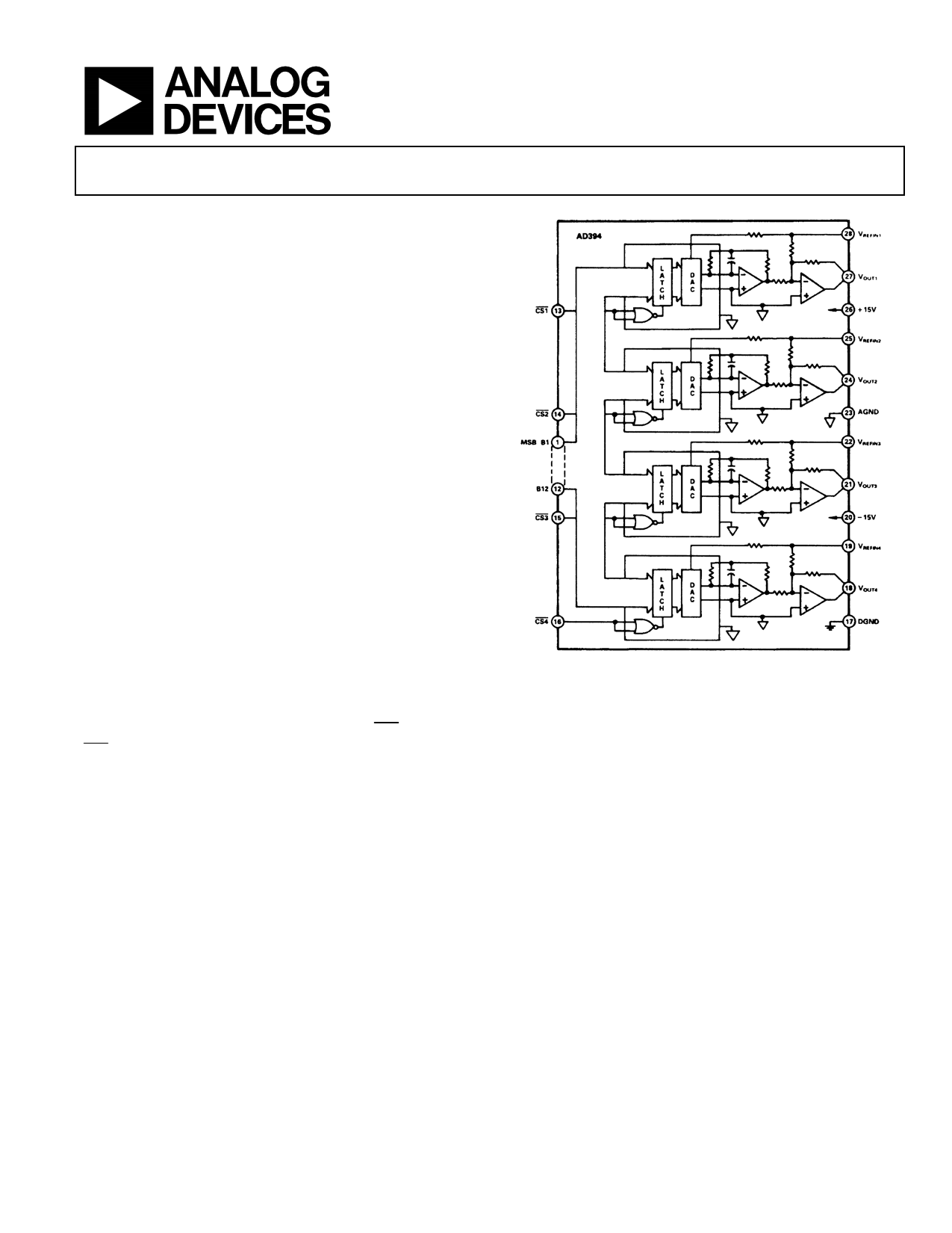
Figure 1. Functional Block Diagram
PRODUCT HIGHLIGHTS
The individual DAC registers are accessed by the CS1 through
CS4 control pins. These control signals allow any combination
of the DAC select matrix to occur (see Table 3). Once selected,
the DAC is loaded with a single 12-bit wide word. The 12-bit
parallel digital input interfaces to most 12- and 16-bit bus
systems.
1. The AD394 offers a dramatic reduction in printed circuit
board space in systems using multiple low power DACs.
2. Each DAC is independently addressable and provides
versatile control architecture for a simple interface to
microprocessors. All latch enable signals are level-
triggered.
The AD394 outputs (VREFIN = 10 V) provide a ±10 V bipolar
output range with positive-true offset binary input coding.
3. The output voltage is trimmed to a full-scale accuracy of
±0.05%. Settling time to ±1/2 LSB is 15 µs maximum.
The AD394 is packaged in a 28-lead ceramic package and is
available for operation over a −55°C to +125°C temperature
range.
4. A maximum gain TC of 5 ppm/°C is achievable.
5. Two- or four-quadrant multiplication can be achieved
simply by applying the appropriate input voltage signal to
the selected DAC's reference (VREFIN).
6. The AD394TD features guaranteed accuracy and linearity
over the −55°C to +125°C temperature range.
Rev. A
Information furnished by Analog Devices is believed to be accurate and reliable.
However, no responsibility is assumed by Analog Devices for its use, nor for any
infringements of patents or other rights of third parties that may result from its use.
Specifications subject to change without notice. No license is granted by implication
or otherwise under any patent or patent rights of Analog Devices. Trademarks and
registered trademarks are the property of their respective owners.
One Technology Way, P.O. Box 9106, Norwood, MA 02062-9106, U.S.A.
Tel: 781.329.4700
www.analog.com
Fax: 781.326.8703 © 2004 Analog Devices, Inc. All rights reserved.
1 page 
AD394
ABSOLUTE MAXIMUM RATINGS
Table 2.
Parameter
+VS to DGND
−VS to DGND
Digital Inputs (Pins 1-16) to DNGD
VREFIN to DGND
AGND to DGND
Rating
−0.3 V to +17 V
−17 V to +0.3 V
−0.3 V to +7 V
±25 V
±0.6 V
Stresses above those listed under “Absolute Maximum Ratings”
may cause permanent damage to the device. This is a stress
rating only and functional operation at or above this specifica-
tion is not implied. Exposure to above maximum rating
conditions for extended periods may affect device reliability.
Analog Output (Pins 18, 21, 24, 27) Indefinite short to AGND
or DGND momentary
short to ±VS
ESD CAUTION
ESD (electrostatic discharge) sensitive device. Electrostatic charges as high as 4000 V readily accumulate on
the human body and test equipment and can discharge without detection. Although this product features
proprietary ESD protection circuitry, permanent damage may occur on devices subjected to high energy
Oelectrostatic discharges. Therefore, proper ESD precautions are recommended to avoid performance
degradation or loss of functionality.
BSOLMIL-STD-883
EThe rigors of the military and aerospace environment, temp-
erature extremes, humidity, mechanical stress, etc., demand the
TEutmost in electronic circuits. The AD394, with the inherent
reliability of an integrated circuit construction, was designed
with these applications in mind. The hermetically-sealed, low
profile DIP package takes up a fraction of the space required by
equivalent modular designs and protects the chips from
hazardous environments. To further insure reliability, the
AD394 is fully compliant to MIL-STD-833 Class B, Method
5008.
Figure 2. Feedthrough VREFIN = 60 Hz (Top Photo) and 400 Hz (Bottom Photo).
The Sine-Wave Digital Code Is Set at 1000 000 0000. Scale: Reference Input Is
5 V/DIV (Thin Trace). Feedthrough Output Is 5 mV/DIV. Time: 5 ms/DIV (Top
Photo), 500 µs/DIV (Bottom Photo).
Rev. A | Page 5 of 12
5 Page 
AD394
OR’ed with LED indicators as shown. The test limits for each
comparator are programmed by the AD394 VOUT2 and VOUT3
outputs. When the output of the device under testing is within
the limits, both comparators are off and D1 lights. If the output
is above or below the limits, either D4 or D5 lights.
code is applied to the DAC; the output voltage is the product of
the two—an attenuated version of the input. The maximum
attenuation range obtainable utilizing 12 bits is 4096:1 or 72 dB.
AD394 as a Multiplier and Attenuator
So far, it has been assumed that the reference voltage VREFIN is
fixed. In fact, VREFIN can be any voltage within the range of
−11 V < VREFIN < +11 V. It can be negative, positive, sinusoidal, or
whatever the user prefers. This leads to the name “multiplying
D/A converters” because the output voltage, VOUT, is propor-
tional to the product of the digital input word and the voltage at
the VREFIN terminal.
( )VOUT = − 1 VREFIN
D
(4096 )
(0 < D < 4095)
D is the fractional binary value of the digital word applied to the
Oconverter. The AD394 multiplies the digital input value by the
analog input voltage at VREFIN for any value of VREFIN up to
B22 V p-p. This in itself is a powerful tool. Applications requiring
Sprecision multiplication with minimal zero offset and very low
distortion should consider the AD394 as a candidate. One pop-
Oular use for the AD394 is as an audio frequency attenuator. The
LETEaudio signal is applied to the VREFIN input and the attenuation
Figure 16. AD394 as a Multiplier or Attenuator
Rev. A | Page 11 of 12
11 Page | ||
| Páginas | Total 12 Páginas | |
| PDF Descargar | [ Datasheet AD394.PDF ] | |
Hoja de datos destacado
| Número de pieza | Descripción | Fabricantes |
| AD390 | Quad 12-Bit Microprocessor-Compatible D/A Converter | Analog Devices |
| AD392 | Complete Quad 12-Bit D/A Converter | Analog Devices |
| AD394 | uP-Compatible Multiplying Quad 12-Bit D/A Converter | Analog Devices |
| AD395 | uP Compatible Multiplying Quad 12-Bit D/A Converter | Analog Devices |
| Número de pieza | Descripción | Fabricantes |
| SLA6805M | High Voltage 3 phase Motor Driver IC. |
Sanken |
| SDC1742 | 12- and 14-Bit Hybrid Synchro / Resolver-to-Digital Converters. |
Analog Devices |
|
DataSheet.es es una pagina web que funciona como un repositorio de manuales o hoja de datos de muchos de los productos más populares, |
| DataSheet.es | 2020 | Privacy Policy | Contacto | Buscar |