|
|
|
PDF 8T39S04A Data sheet ( Hoja de datos )
| Número de pieza | 8T39S04A | |
| Descripción | Crystal or Differential to Differential Clock Fanout Buffer | |
| Fabricantes | IDT | |
| Logotipo | ||
Hay una vista previa y un enlace de descarga de 8T39S04A (archivo pdf) en la parte inferior de esta página. Total 30 Páginas | ||
|
No Preview Available !
Crystal or Differential to
Differential Clock Fanout Buffer
8T39S04A
Datasheet
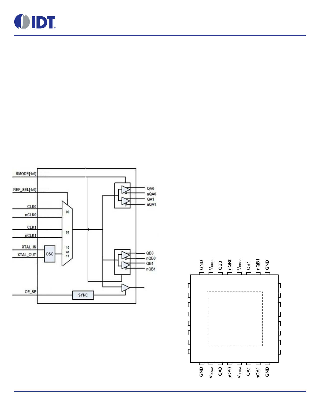
General Description
The 8T39S04A is a high-performance clock fanout buffer. The input
clock can be selected from two differential inputs or one crystal input.
The internal oscillator circuit is automatically disabled if the crystal
input is not selected. The crystal pin can be driven by a single-ended
clock.The selected signal is distributed to four differential outputs
which can be configured as LVPECL, LVDS or HSCL outputs. In
addition, an LVCMOS output is provided. All outputs can be disabled
into a high-impedance state. The device is designed for a signal
fanout of high-frequency, low phase-noise clock and data signal. The
outputs are at a defined level when inputs are open or tied to ground.
It is designed to operate from a 3.3V or 2.5V core power supply, and
either a 3.3V or 2.5V output operating supply.
Block Diagram
PullDown
PullDown
Features
• Two differential reference clock input pairs
• Differential input pairs can accept the following input levels:
LVPECL, LVDS, HCSL, HSTL and Single-ended
• Crystal Oscillator Interface
• Crystal input frequency range: 10MHz to 40MHz
• Maximum Output Frequency
LVPECL - 2GHz
LVDS - 2GHz
HCSL - 250MHz
LVCMOS - 250MHz
• Two banks, each has two differential output pairs that can be
configured as LVPECL or LVDS or HCSL
• One single-ended reference output with synchronous enable to
avoid clock glitch
• Output skew: 80ps (maximum), Bank A and Bank B at the same
output level
• Part-to-part skew: 200ps (typical), design target
• Additive RMS phase jitter @ 156.25MHz, (12kHz - 20MHz):
34.7fs (typical), 3.3V/ 3.3V
• Supply voltage modes:
VDD/VDDO
3.3V/3.3V
3.3V/2.5V
2.5V/2.5V
• -40°C to 85°C ambient operating temperature
• Lead-free (RoHS 6) packaging
Pin Assignment
REFOUT
24 23 22 21 20 19 18 17
nc 25
16
nCLK1 26
15
CLK1 27
14
VDD 28
REFOUT 29
8T39S04A
13
12
VDDOREF 30
11
OE_SE 31
10
SMODE1 32
9
12345678
REF_SEL1
nCLK0
CLK0
REF_SEL0
XTAL_OUT
XTAL_IN
VDD
SMODE0
©2016 Integrated Device Technology, Inc.
32-pin, 5mm x 5mm VFQFN Package
1 May 20, 2016
1 page 
Table 3E. Input/Output Operation Table, SMODE[1:0]
Input Status
SMODE[1:0]
11
00, 01 or 10
REF_SEL[1:0]
Don’t care
10 or 11
CLKx and nCLKx
Don’t Care
Don’t Care
CLK0 and nCLK0 are both open circuit
00, 01 or 10
00 (default)
CLK0 and nCLK0 are tied to ground
CLK0 is high, nCLK0 is low
CLK0 is low, nCLK0 is high
CLK1 and nCLK1 are both open circuit
00, 01 or 10
01
CLK1 and CLK1 are tied to ground.
CLK1 is high, nCLK1 is low
CLK1 is low, nCLK1 is high
Table 3F. Input/Output Operation Table, SMODE[1:0]
Input Status
SMODE[1:0]
11
00, 01 or 10
REF_SEL[1:0]
Don’t care
10 or 11
CLKx and nCLKx
Don’t Care
Don’t Care
CLK0 and nCLK0 are both open circuit
00, 01 or 10
00 (default)
CLK0 and nCLK0 are tied to ground
CLK0 is high, nCLK0 is low
CLK0 is low, nCLK0 is high
CLK1 and nCLK1 are both open circuit
00, 01 or 10
01
CLK1 and nCLK1 are tied to ground
CLK1 is high, nCLK1 is low
CLK1 is low, nCLK1 is high
©2016 Integrated Device Technology, Inc.
5
8T39S04A Datasheet
Output State
QA[1:0], nQA[1:0]
High Impedance
Fanout crystal oscillator
QA[1:0] = Low
nQA[1:0] = High
QA[1:0] = Low
nQA[1:0] = High
QA[1:0] = High
nQA[1:0] = Low
QA[1:0] = Low
nQA[1:0] = High
QA[1:0] = Low
nQA[1:0] = High
QA[1:0] = Low
nQA[1:0] = High
QA[1:0] = High
nQA[1:0] = Low
QA[1:0] = Low
nQA[1:0] = High
Output State
QB[1:0], nQB[1:0]
High Impedance
Fanout Crystal Oscillator
QB[1:0] = Low
nQB[1:0] = High
QB[1:0] = Low
nQB[1:0] = High
QB[1:0] = High
nQB[1:0] = Low
QB[1:0] = Low
nQB[1:0] = High
QB[1:0] = Low
nQB[1:0] = High
QB[1:0] = Low
nQB[1:0] = High
QB[1:0] = High
nQB[1:0] = Low
QB[1:0] = Low
nQB[1:0] = High
May 20, 2016
5 Page 
8T39S04A Datasheet
NOTE 6. This parameter is defined in accordance with JEDEC Standard 65.
NOTE 7. Defined as skew between outputs on different devices operating at the same supply voltage, same temperature, same frequency
and with equal load conditions. Using the same type of inputs on each device, the outputs are measured at the differential cross-
point.
NOTE 8. Measurement taken from single-ended waveform.
NOTE 9. Defined as the maximum instantaneous voltage including overshoot.
NOTE 10. Defined as the minimum instantaneous voltage including undershoot.
NOTE 11. Measured at crosspoint where the instantaneous voltage value of the rising edge of Qx equals the falling edge of nQx.
NOTE 12. Refers to the total variation from the lowest crosspoint to the highest, regardless of which edge is crossing. Refers to all crosspoint
for this measurement.
NOTE 13. Defined as the total variation of all crossing voltages of rising Qx and falling nQx, This is the maximum allowed variance in Vcross
for any particular system.
NOTE 14. Measured from -150mV to +150mV on the differential waveform (Qx minus nQx). The signal must be monotonic through the mea-
surement region for rise and fall time. The 300mV measurement window is centered on the differential zero crossing.
NOTE 15. Measured at 100MHz.
NOTE 16. Measured for the following frequencies: 25MHz, 100MHz, 125MHz, 156.25MHz, 312.5MHz, 400MHz, and 644.5313MHz.
©2016 Integrated Device Technology, Inc.
11
May 20, 2016
11 Page | ||
| Páginas | Total 30 Páginas | |
| PDF Descargar | [ Datasheet 8T39S04A.PDF ] | |
Hoja de datos destacado
| Número de pieza | Descripción | Fabricantes |
| 8T39S04A | Crystal or Differential to Differential Clock Fanout Buffer | IDT |
| Número de pieza | Descripción | Fabricantes |
| SLA6805M | High Voltage 3 phase Motor Driver IC. |
Sanken |
| SDC1742 | 12- and 14-Bit Hybrid Synchro / Resolver-to-Digital Converters. |
Analog Devices |
|
DataSheet.es es una pagina web que funciona como un repositorio de manuales o hoja de datos de muchos de los productos más populares, |
| DataSheet.es | 2020 | Privacy Policy | Contacto | Buscar |