|
|
|
PDF 8L30110 Data sheet ( Hoja de datos )
| Número de pieza | 8L30110 | |
| Descripción | Crystal or Differential to LVCMOS/LVTTL Clock Buffer | |
| Fabricantes | IDT | |
| Logotipo | ||
Hay una vista previa y un enlace de descarga de 8L30110 (archivo pdf) en la parte inferior de esta página. Total 22 Páginas | ||
|
No Preview Available !
Crystal or Differential to LVCMOS/ LVTTL
Clock Buffer
8L30110
Datasheet
General Description
The 8L30110 is a low skew, 1-to-10 LVCMOS / LVTTL Fanout Buffer.
The low impedance LVCMOS/LVTTL outputs are designed to drive
50 series or parallel terminated transmission lines.
The 8L30110 is characterized at full 3.3V and 2.5V, mixed 3.3V/2.5V,
3.3V/1.8V, 3.3V/1.5V, 2.5V/1.8V and 2.5V/1.5V output operating
supply modes. The input clock is selected from two differential clock
inputs or a crystal input. The differential input can be wired to accept
a single-ended input. The internal oscillator circuit is automatically
disabled if the crystal input is not selected.
Features
• Ten LVCMOS / LVTTL outputs up to 200MHz
• Differential input pair can accept the following differential input
levels: LVPECL, LVDS, HCSL
• Crystal Oscillator Interface
• Crystal input frequency range: 8MHz to 50MHz
• Output skew: 63ps (typical)
• Additive RMS phase jitter: 22fs (typical)
• Power supply modes:
Core / Output
3.3V / 3.3V
3.3V / 2.5V
3.3V / 1.8V
3.3V / 1.5V
2.5V / 2.5V
2.5V / 1.8V
2.5V / 1.5V
• -40°C to 85°C ambient operating temperature
• Lead-free (RoHS 6) packaging
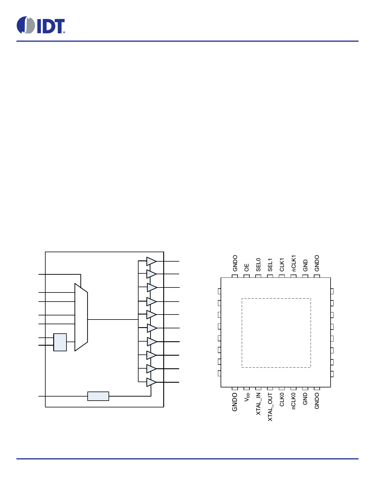
Block Diagram
Pin Assignment
SEL[1: 0]
Pulldown
CLK0
nCLK0
CLK1
nCLK1
XTAL_OUT
XTAL_IN
Pulldown
Pullup/ Pulldown
00
Pulldown
Pullup/ Pulldown
01
OSC
1x
OE Pulldown
SYNC
Q0
Q1
Q2 32 31 30 29 28 27 26 25
Q0 1
Q3
VDDO 2
24 Q9
23 VDDO
Q4 Q1 3
22 Q8
Q5 GNDO 4
Q6 Q2 5
8L30110
21 GNDO
20 Q7
Q7 VDDO 6
19 VDDO
Q3 7
Q8
18 Q6
Q4 8
17 Q5
Q9
9 10 11 12 13 14 15 16
©2016 Integrated Device Technology, Inc.
32-pin, 5mm x 5mm VFQFN Package
1 Revision 3, February 18, 2016
1 page 
8L30110 Datasheet
:
Table 4C. LVCMOS/LVTTL DC Characteristics,
VDD = 3.3V±5% or 2.5V±5%, VDDO (VDD) = 3.3V±5% or 2.5V±5% or 1.8V±0.2V or 1.5V±0.15V, TA = -40°C to 85°C
Symbol Parameter
Test Conditions
Minimum
Typical
Maximum
VIH Input High Voltage
VIL Input Low Voltage
IIH
Input High
Current
OE, SEL[1:0]
VDD = 3.3V±5%
VDD = 2.5V±5%
VDD = 3.3V±5%
VDD = 2.5V±5%
VDD = VIN = 3.465V
2
1.7
0.8
0.7
150
IIL
Input Low
Current
OE, SEL[1:0]
VDD = 3.465V, VIN = 0V
-5
VOH Output High Voltage
VOL Output Low Voltage
VDDO = 3.3V±5%, IOH = -12mA
VDDO = 2.5V±5%, IOH = -8mA
VDDO = 1.8V±0.2V, IOH = -2mA
VDDO = 1.5V±0.15V, IOH = -2mA
VDDO = 3.3V±5%, IOL = 12mA
VDDO = 2.5V±5%, IOL = 8mA
VDDO = 1.8V±0.2V, IOL = 2mA
VDDO = 1.5V±0.15V, IOL = 2mA
2.6
1.8
1.2
0.95
0.5
0.5
0.4
0.35
Units
V
V
V
V
µA
µA
V
V
V
V
V
V
V
V
Table 4D. Differential DC Characteristics,
VDD = 3.3V±5% or 2.5V±5%, VDDO (VDD) = 3.3V±5% or 2.5V±5% or 1.8V±0.2V or 1.5V±0.15V, TA = -40°C to 85°C
Symbol Parameter
Test Conditions
Minimum Typical Maximum
IIH
Input High
Current
CLK[0:1],
nCLK[0:1]
VDD = VIN = 3.465V or 2.625V
150
IIL
VPP
VCMR
Input Low
Current
CLK[0:1]
nCLK[0:1]
Peak-to-Peak Input Voltage1
Common Mode Input Voltage 1, 2
VDD = 3.465V or 2.625V, VIN = 0V
VDD = 3.465V or 2.625V,VIN = 0V
NOTE 1. VIL should not be less than -0.3V and VIH should not be greater than VDD.
NOTE 2. Common mode voltage is defined at the crosspoint.
-5
-150
0.15
0.5
1.3
VDD – 0.85
Units
µA
µA
µA
V
V
Table 5. Crystal Characteristics1
Parameter
Test Conditions
Minimum
Mode of Oscillation
Frequency
8
Equivalent Series Resistance (ESR)
Shunt Capacitance
Load Capacitance (CL)
NOTE 1. To insure crystal accuracy, the use of external tuning capacitors is required.
Typical
Fundamental
12
Maximum
50
50
7
18
Units
MHz
pF
pF
©2016 Integrated Device Technology, Inc.
5
Revision 3, February 18, 2016
5 Page 
8L30110 Datasheet
Wiring the Differential Input to Accept Single-Ended Levels
Figure 2 shows how a differential input can be wired to accept single
ended levels. The reference voltage V1= VDD/2 is generated by the
bias resistors R1 and R2. The bypass capacitor (C1) is used to help
filter noise on the DC bias. This bias circuit should be located as close
to the input pin as possible. The ratio of R1 and R2 might need to be
adjusted to position the V1in the center of the input voltage swing. For
example, if the input clock is driven from a single-ended 2.5V
LVCMOS driver and the DC offset (or swing center) of this signal is
1.25V, the R1 and R2 values should be adjusted to set the V1 at
1.25V. The values below are for when both the single ended swing
and VDD are at the same voltage. This configuration requires that the
sum of the output impedance of the driver (Ro) and the series
resistance (Rs) equals the transmission line impedance. In addition,
matched termination at the input will attenuate the signal in half. This
can be done in one of two ways. First, R3 and R4 in parallel should
equal the transmission line impedance. For most 50 applications,
R3 and R4 can be 100. The values of the resistors can be increased
to reduce the loading for slower and weaker LVCMOS driver. When
using single-ended signaling, the noise rejection benefits of
differential signaling are reduced. Even though the differential input
can handle full rail LVCMOS signaling, it is recommended that the
amplitude be reduced while maintaining an edge rate faster than
1V/ns. The datasheet specifies a lower differential amplitude,
however this only applies to differential signals. For single-ended
applications, the swing can be larger, however VIL cannot be less
than -0.3V and VIH cannot be more than VDD + 0.3V. Though some
of the recommended components might not be used, the pads
should be placed in the layout. They can be utilized for debugging
purposes. The datasheet specifications are characterized and
guaranteed by using a differential signal.
Figure 2. Recommended Schematic for Wiring a Differential Input to Accept Single-ended Levels
Crystal Input Interface
The 8L30110 has been characterized with 12pF parallel resonant
crystals. The capacitor values, C1 and C2, shown in Figure 3 below
were determined using an 12pF parallel resonant crystal and were
chosen to minimize the ppm error. The optimum C1 and C2 values
can be slightly adjusted for different board layouts.
X1
12pF Parallel Crystal
C1
10pF
XTAL_IN
C2
10pF
XTAL_OUT
Figure 3. Crystal Input Interface
©2016 Integrated Device Technology, Inc.
11
Revision 3, February 18, 2016
11 Page | ||
| Páginas | Total 22 Páginas | |
| PDF Descargar | [ Datasheet 8L30110.PDF ] | |
Hoja de datos destacado
| Número de pieza | Descripción | Fabricantes |
| 8L30110 | Crystal or Differential to LVCMOS/LVTTL Clock Buffer | IDT |
| Número de pieza | Descripción | Fabricantes |
| SLA6805M | High Voltage 3 phase Motor Driver IC. |
Sanken |
| SDC1742 | 12- and 14-Bit Hybrid Synchro / Resolver-to-Digital Converters. |
Analog Devices |
|
DataSheet.es es una pagina web que funciona como un repositorio de manuales o hoja de datos de muchos de los productos más populares, |
| DataSheet.es | 2020 | Privacy Policy | Contacto | Buscar |