|
|
|
PDF 8530I-01 Data sheet ( Hoja de datos )
| Número de pieza | 8530I-01 | |
| Descripción | 1-to-16 Differential-to-3.3V LVPECL Fanout Buffer | |
| Fabricantes | IDT | |
| Logotipo | ||
Hay una vista previa y un enlace de descarga de 8530I-01 (archivo pdf) en la parte inferior de esta página. Total 18 Páginas | ||
|
No Preview Available !
Low Skew, 1-to-16 Differential-to-3.3V
LVPECL Fanout Buffer
8530I-01
Datasheet
General Description
The 8530I-01is a low skew, 1-to-16 Differential- to-3.3V LVPECL
Fanout Buffer. The CLK, nCLK pair can accept most standard
differential input levels. The high gain differential amplifier accepts
peak-to-peak input voltages as small as 150mV as long as the
common mode voltage is within the specified minimum and
maximum range.
Guaranteed output and part-to-part skew characteristics make the
8530I-01 ideal for those clock distribution applications demanding
well defined performance and repeatability.
Features
• Sixteen differential 3.3V LVPECL output pairs
• CLK, nCLK input pair
• CLK, nCLK pair can accept the following differential input
levels: LVPECL, LVDS, LVHSTL, HCSL, SSTL
• Maximum output frequency: 500MHz
• Translates any single-ended input signal to 3.3V LVPECL levels
with a resistor bias on nCLK input
• Output skew: 75ps (maximum)
• Additive phase jitter, RMS @ 106.25MHz: 0.162ps (typical)
• Full 3.3V supply voltage
• -40°C to 85°C ambient operating temperature
• Available in lead-free (RoHS 6) package
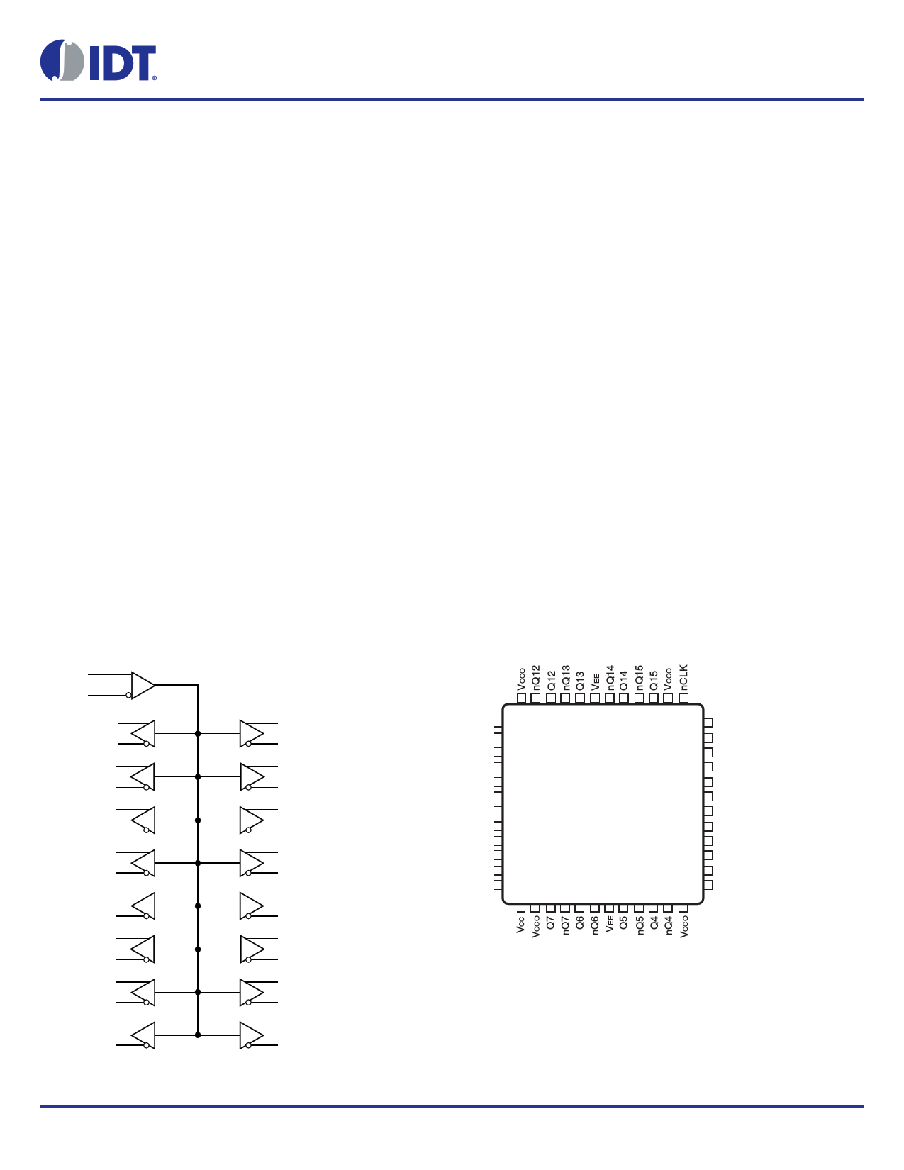
Block Diagram
CLK0 Pulldown
nCLK0 Pullup
Q0
nQ0
Q1
nQ1
Q2
nQ2
Q3
nQ3
Q4
nQ4
Q5
nQ5
Q6
nQ6
Q7
nQ7
Q15
nQ15
Q14
nQ14
Q13
nQ13
Q12
nQ12
Q11
nQ11
Q10
nQ10
Q9
nQ9
Q8
nQ8
©2015 Integrated Device Technology, Inc.
Pin Assignment
VCCO
Q11
nQ11
Q10
nQ10
VEE
Q9
nQ9
Q8
nQ8
VCCO
VCC
48 47 46 45 44 43 42 41 40 39 38 37
1 36
2 35
3 34
4 33
5 32
6 31
7 30
8 29
9 28
10 27
11 26
12 25
13 14 15 16 17 18 19 20 21 22 23 24
CLK
VCCO
nQ0
Q0
nQ1
Q1
VEE
nQ2
Q2
nQ3
Q3
VCCO
8530I-01
48-Lead TQFP, E-Pad
7mm x 7mm x 1.0mm package body
Y Package
Top View
1 Revision B, December 1, 2015
1 page 
8530I-01 Datasheet
Additive Phase Jitter
The spectral purity in a band at a specific offset from the fundamental
compared to the power of the fundamental is called the dBc Phase
Noise. This value is normally expressed using a Phase noise plot
and is most often the specified plot in many applications. Phase
noise is defined as the ratio of the noise power present in a 1Hz band
at a specified offset from the fundamental frequency to the power
value of the fundamental. This ratio is expressed in decibels (dBm)
or a ratio of the power in the 1Hz band to the power in the
fundamental. When the required offset is specified, the phase noise
is called a dBc value, which simply means dBm at a specified offset
from the fundamental. By investigating jitter in the frequency domain,
we get a better understanding of its effects on the desired application
over the entire time record of the signal. It is mathematically possible
to calculate an expected bit error rate given a phase noise plot.
Additive Phase Jitter @ 106.25MHz
12kHz to 20MHz = 0.162ps (typical)
Offset from Carrier Frequency (Hz)
As with most timing specifications, phase noise measurements has
issues relating to the limitations of the equipment. Often the noise
floor of the equipment is higher than the noise floor of the device. This
is illustrated above. The device meets the noise floor of what is
shown, but can actually be lower. The phase noise is dependent on
the input source and measurement equipment.
©2015 Integrated Device Technology, Inc.
5
Revision B, December 1, 2015
5 Page 
8530I-01 Datasheet
Termination for 3.3V LVPECL Outputs
The clock layout topology shown below is a typical termination for
LVPECL outputs. The two different layouts mentioned are
recommended only as guidelines.
Differential outputs are low impedance follower outputs that generate
ECL/LVPECL compatible outputs. Therefore, terminating resistors
(DC current path to ground) or current sources must be used for
functionality. These outputs are designed to drive 50 transmission
lines. Matched impedance techniques should be used to maximize
operating frequency and minimize signal distortion. Figures 4A and
4B show two different layouts which are recommended only as
guidelines. Other suitable clock layouts may exist and it would be
recommended that the board designers simulate to guarantee
compatibility across all printed circuit and clock component process
variations.
3.3V
3.3V
R3 R4
125
125
3.3V
Zo = 50
+
Zo = 50
R1
84
_
R2
84
Input
Figure 4A. 3.3V LVPECL Output Termination
Figure 4B. 3.3V LVPECL Output Termination
©2015 Integrated Device Technology, Inc.
11
Revision B, December 1, 2015
11 Page | ||
| Páginas | Total 18 Páginas | |
| PDF Descargar | [ Datasheet 8530I-01.PDF ] | |
Hoja de datos destacado
| Número de pieza | Descripción | Fabricantes |
| 8530I-01 | 1-to-16 Differential-to-3.3V LVPECL Fanout Buffer | IDT |
| Número de pieza | Descripción | Fabricantes |
| SLA6805M | High Voltage 3 phase Motor Driver IC. |
Sanken |
| SDC1742 | 12- and 14-Bit Hybrid Synchro / Resolver-to-Digital Converters. |
Analog Devices |
|
DataSheet.es es una pagina web que funciona como un repositorio de manuales o hoja de datos de muchos de los productos más populares, |
| DataSheet.es | 2020 | Privacy Policy | Contacto | Buscar |