|
|
|
PDF 9DBU0641 Data sheet ( Hoja de datos )
| Número de pieza | 9DBU0641 | |
| Descripción | 6 O/P 1.5V PCIe Gen1-2-3 ZDB/FOB | |
| Fabricantes | IDT | |
| Logotipo | ||
Hay una vista previa y un enlace de descarga de 9DBU0641 (archivo pdf) en la parte inferior de esta página. Total 17 Páginas | ||
|
No Preview Available !
6 O/P 1.5V PCIe Gen1-2-3 ZDB/FOB
w/Zo=100ohms
9DBU0641
DATASHEET
Description
The 9DBU0641 is a member of IDT's 1.5V Ultra-Low-Power
(ULP) PCIe family. It has integrated output terminations
providing Zo=100 for direct connection to 100
transmission lines. The device has 6 output enables for clock
management and 3 selectable SMBus addresses.
Recommended Application
1.5V PCIe Gen1-2-3 Zero Delay/Fanout Buffer (ZDB/FOB)
Output Features
• 6 – 1-167MHz Low-Power (LP) HCSL DIF pairs
w/Zo=100
Key Specifications
• DIF cycle-to-cycle jitter <50ps
• DIF output-to-output skew <60ps
• DIF phase jitter is PCIe Gen1-2-3 compliant
• DIF bypass mode additive phase jitter is <300fs rms for
PCIe Gen3
• DIF bypass mode additive phase jitter <350fs rms for
12k-20MHz
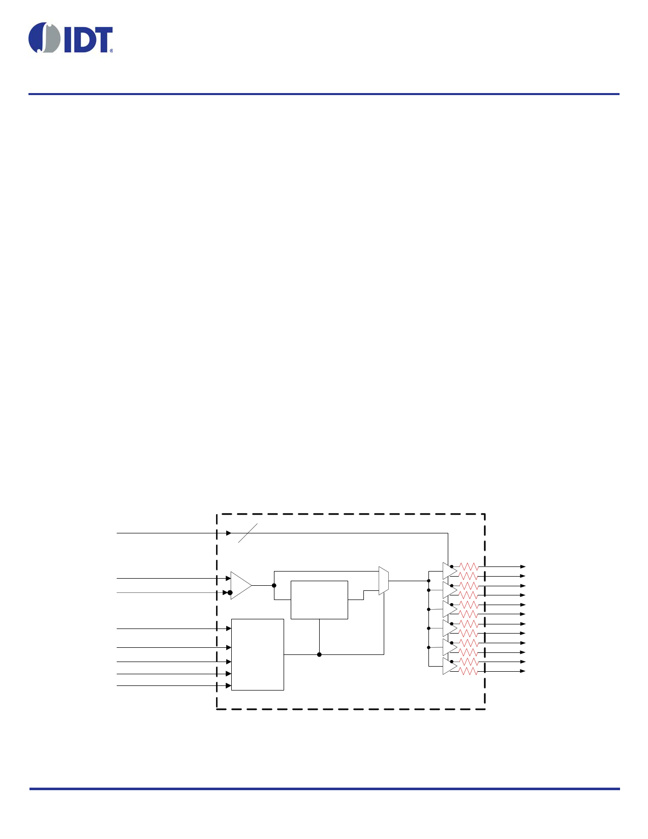
Block Diagram
vOE(5:0)#
6
Features/Benefits
• Direct connection to 100 transmission lines; saves 24
resistors compared to standard HCSL outputs
• 46mW typical power consumption in PLL mode; eliminates
thermal concerns
• Outputs can optionally be supplied from any voltage
between 1.05 and 1.5V; maximum power savings
• Spread Spectrum (SS) compatible; allows SS for EMI
reduction
• OE# pins; support DIF power management
• HCSL-compatible differential input; can be driven by
common clock sources
• SMBus-selectable features; optimize signal integrity to
application
• slew rate for each output
• differential output amplitude
• Pin/SMBus selectable PLL bandwidth and PLL Bypass;
optimze PLL to application
• Outputs blocked until PLL is locked; clean system start-up
• Device contains default configuration; SMBus interface not
required for device control
• 3.3V tolerant SMBus interface works with legacy controllers
• Three selectable SMBus addresses; multiple devices can
easily share an SMBus segment
• Space saving 40-pin 5x5mm VFQFPN; minimal board
space
CLK_IN
CLK_IN#
vSADR
^vHIBW_BYPM_LOBW#
^CKPWRGD_PD#
SDATA_3.3
SCLK_3.3
SS-
Compatible
PLL
CONTROL
LOGIC
DIF5
DIF4
DIF3
DIF2
DIF1
DIF0
9DBU0641 REVISION C 04/22/15
1
©2015 Integrated Device Technology, Inc.
1 page 
9DBU0641 DATASHEET
Absolute Maximum Ratings
Stresses above the ratings listed below can cause permanent damage to the 9DBU0641. These ratings, which are standard
values for IDT commercially rated parts, are stress ratings only. Functional operation of the device at these or any other
conditions above those indicated in the operational sections of the specifications is not implied. Exposure to absolute maximum
rating conditions for extended periods can affect product reliability. Electrical parameters are guaranteed only over the
recommended operating temperature range.
PARAMETER
SYMBOL
CONDITIONS
Supply Voltage
VDDx
Input Voltage
VIN
Input High Voltage, SMBus VIHSMB
Storage Temperature
Ts
SMBus clock and data pins
Junction Temperature
Tj
Input ESD protection
ESD prot
Human Body Model
1Guaranteed by design and characterization, not 100% tested in production.
2 Operation under these conditions is neither implied nor guaranteed.
3 Not to exceed 2.0V.
MIN
-0.5
-0.5
-65
2000
TYP
MAX
2
VDD+0.5
3.3
150
125
UNITS NOTES
V 1,2
V 1,3
V1
°C 1
°C 1
V1
Electrical Characteristics–Clock Input Parameters
TA = TAMB, Supply Voltages per normal operation conditions, See Test Loads for Loading Conditions
PARAMETER
SYMBOL
CONDITIONS
MIN
Input Common Mode
Voltage - DIF_IN
VCOM
Common Mode Input Voltage
200
Input Swing - DIF_IN
Input Slew Rate - DIF_IN
VSWING
dv/dt
Differential value
Measured differentially
300
0.4
Input Leakage Current
IIN
VIN = VDD , VIN = GND
Input Duty Cycle dtin Measurement from differential wavefrom
Input Jitter - Cycle to Cycle JDIFIn
Differential Measurement
1 Guaranteed by design and characterization, not 100% tested in production.
2 Slew rate measured through +/-75mV window centered around differential zero
-5
45
0
TYP
50
MAX
725
1450
8
5
55
150
UNITS NOTES
mV 1
mV
V/ns
uA
%
ps
1
1,2
1
1
REVISION C 04/22/15
5 6 O/P 1.5V PCIE GEN1-2-3 ZDB/FOB W/ZO=100OHMS
5 Page 
9DBU0641 DATASHEET
SMBus Table: Output Enable Register 1
Byte 0
Name
Control Function
Type
0
Bit 7
DIF OE5
Output Enable
RW Low/Low
Bit 6
DIF OE4
Output Enable
RW Low/Low
Bit 5
Reserved
Bit 4
DIF OE3
Output Enable
RW Low/Low
Bit 3
DIF OE2
Output Enable
RW Low/Low
Bit 2
DIF OE1
Output Enable
RW Low/Low
Bit 1
Reserved
Bit 0
DIF OE0
Output Enable
RW Low/Low
1. A low on these bits will overide the OE# pin and force the differential output Low/Low
1
Enabled
Enabled
Enabled
Enabled
Enabled
Enabled
Default
1
1
1
1
1
1
1
1
SMBus Table: PLL Operating Mode and Output Amplitude Control Register
Byte 1
Name
Control Function
Type
0
1
Bit 7
Bit 6
PLLMODERB1
PLLMODERB0
PLL Mode Readback Bit 1
PLL Mode Readback Bit 0
R
R
See PLL Operating Mode Table
Bit 5
PLLMODE_SWCNTRL
Enable SW control of PLL
Mode:
RW Values in B1[7:6] Values in B1[4:3]
set PLL Mode
set PLL Mode
Bit 4
Bit 3
PLLMODE1
PLLMODE0
PLL Mode Control Bit 1
PLL Mode Control Bit 0
RW1
RW1
See PLL Operating Mode Table
Bit 2
Reserved
Bit 1
Bit 0
AMPLITUDE 1
AMPLITUDE 0
Controls Output Amplitude
RW
RW
00 = 0.55V
10 = 0.7V
01= 0.65V
11 = 0.8V
1. B1[5] must be set to a 1 for these bits to have any effect on the part.
Default
Latch
Latch
0
0
0
1
1
0
SMBus Table: DIF Slew Rate Control Register
Byte 2
Name
Control Function
Bit 7
SLEWRATESEL DIF5
Adjust Slew Rate of DIF5
Bit 6
SLEWRATESEL DIF4
Adjust Slew Rate of DIF4
Bit 5
Reserved
Bit 4
SLEWRATESEL DIF3
Adjust Slew Rate of DIF3
Bit 3
SLEWRATESEL DIF2
Adjust Slew Rate of DIF2
Bit 2
SLEWRATESEL DIF1
Adjust Slew Rate of DIF1
Bit 1
Reserved
Bit 0
SLEWRATESEL DIF0
Adjust Slew Rate of DIF0
Note: See "Low-Power HCSL Outputs" table for slew rates.
Type
RW
RW
RW
RW
RW
RW
0
Slow Setting
Slow Setting
Slow Setting
Slow Setting
Slow Setting
Slow Setting
1
Fast Setting
Fast Setting
Fast Setting
Fast Setting
Fast Setting
Fast Setting
Default
1
1
1
1
1
1
1
1
SMBus Table: Frequency Select Control Register
Byte 3
Name
Control Function
Bit 7
Reserved
Bit 6
Bit 5
Reserved
Reserved
Bit 4
Reserved
Bit 3
Bit 2
Bit 1
Bit 0
SLEWRATESEL FB
Reserved
Reserved
Reserved
Adjust Slew Rate of FB
Type
RW
0
Slow Setting
1
Fast Setting
Default
1
1
0
0
0
1
1
1
Byte 4 is Reserved and reads back 'hFF
REVISION C 04/22/15
11 6 O/P 1.5V PCIE GEN1-2-3 ZDB/FOB W/ZO=100OHMS
11 Page | ||
| Páginas | Total 17 Páginas | |
| PDF Descargar | [ Datasheet 9DBU0641.PDF ] | |
Hoja de datos destacado
| Número de pieza | Descripción | Fabricantes |
| 9DBU0641 | 6 O/P 1.5V PCIe Gen1-2-3 ZDB/FOB | IDT |
| Número de pieza | Descripción | Fabricantes |
| SLA6805M | High Voltage 3 phase Motor Driver IC. |
Sanken |
| SDC1742 | 12- and 14-Bit Hybrid Synchro / Resolver-to-Digital Converters. |
Analog Devices |
|
DataSheet.es es una pagina web que funciona como un repositorio de manuales o hoja de datos de muchos de los productos más populares, |
| DataSheet.es | 2020 | Privacy Policy | Contacto | Buscar |