|
|
PDF HYM1302 Data sheet ( Hoja de datos )
| Número de pieza | HYM1302 | |
| Descripción | Serial Real Time Clock/Calendar | |
| Fabricantes | Haoyu | |
| Logotipo |  |
|
Hay una vista previa y un enlace de descarga de HYM1302 (archivo pdf) en la parte inferior de esta página. Total 10 Páginas | ||
|
No Preview Available !
HYM1302
HYM1302
Serial Real Time Clock/Calendar
With 31×8 RAM
Data Sheet
Features
■ 31 x 8 RAM for scratchpad data storage
■ Dual power supply pins
■ Serial I/O transmission
■ Clock registers store BCD format
■ Operating voltage: 2.0V-5.5V
■ Uses less than 300 nA at 2.0 volts
■ Two data transmission modes: single-byte,or
burst mode
■ 8–pin DIP or 8–pin SOP package
■ Maximum input serial clock: 500kHz at VCC =2V,
2MHz at VCC =5V
■ TTL–compatible (VCC = 5V)
■ DS1302 compatible
Applications
■ Cash Register
■ Security Access Controller, Door Controller
■ Time Recorder
■ Mobile Telephones
■ Public Phone Bill Meter, Smart Card Payphone
■ MP3/MP4 Player
■ IC Water-Flow Meter, IC Gas Meter
General Description
The HYM1302 is a serial timekeeper IC which
provides seconds, minutes, hours, day, date, month,
and year information. A 32.768KHz crystal is
required to provide the correct timing. The number
of days in each month and leap years are
automatically adjusted. The clock can operate in two
modes: one is the 12-hour mode with an AM/PM
indicator, the other is the 24-hour mode. In addition,
the HYM1302 has additional features of dual power
pins for primary and functions of the back-up power
supplies, programmable trickle charger for VCC1, and
31 bytes of static RAM for scratchpad data storage.
In order to minimize the pin number, The HYM1302
uses a serial I/O transmission method to interface
with a microprocessor. Only three wires are required:
(1) RST (Reset), (2) I/O (Data line), and (3) SCLK
(Serial clock). Data can be transferred to and from
the clock/RAM 1 byte at a time or in a burst of up to
31 bytes. The HYM1302 is designed to operate on
very low power.
Block Diagram and Pin Description
Pin Assignment
HYM1302 (N)—8DIP
HYM1302Z (N) —8SOP
-1-
1 page 
HYM1302
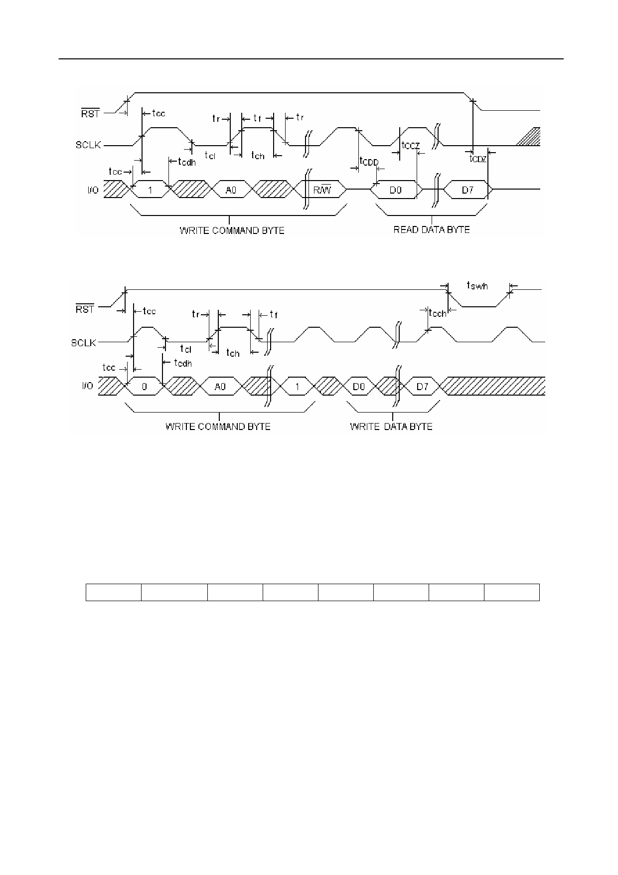
Timing Diagram: Read Data Transfer
Timing Diagram: Write Data Transfer
Application Information
Command Byte
For each data transfer, a command byte is initiated to specify which register is accessed. This is to determine
whether a read or write is operated and whether a single byte or burst mode transfer is to occur. The
command byte is shown in Table 1.
Table 1.Address/ Command Byte
1 R/C A4 A3 A2 A1 A0 R/W
The MSB (Bit 7) must be logic 1. If it is 0, HYM1302 will not be written. R/C (Bit 6) specifies clock/calendar
data if logic 0 or RAM data if logic 1. A4-A0 (Bits 1 through 5) specify the designated registers to be input or
output, and the R/W (bit 0) specifies a write operation if logic 0 or read operation if logic 1. The command byte
is always input starting with the LSB (bit 0).
Clock/Calendar and RAM
The clock/calendar is contained in seven write/read registers. Data contained in the clock/ calendar registers
is in binary coded decimal format (BCD). The static RAM is 31x8 bytes addressed consecutively in the RAM
address space. The registers and data format summary is shown in Table 2.
-5-
5 Page | ||
| Páginas | Total 10 Páginas | |
| PDF Descargar | [ Datasheet HYM1302.PDF ] | |
Hoja de datos destacado
| Número de pieza | Descripción | Fabricantes |
| HYM1302 | High Performance Low Power RAM Real-Time Clock Chip | ETC |
| HYM1302 | Serial Real Time Clock/Calendar | Haoyu |
| Número de pieza | Descripción | Fabricantes |
| SLA6805M | High Voltage 3 phase Motor Driver IC. |
Sanken |
| SDC1742 | 12- and 14-Bit Hybrid Synchro / Resolver-to-Digital Converters. |
Analog Devices |
|
DataSheet.es es una pagina web que funciona como un repositorio de manuales o hoja de datos de muchos de los productos más populares, |
| DataSheet.es | 2020 | Privacy Policy | Contacto | Buscar |
