|
|
|
PDF 9FGU0841 Data sheet ( Hoja de datos )
| Número de pieza | 9FGU0841 | |
| Descripción | 8-output 1.5V PCIe Gen1-2-3 Clock Generator | |
| Fabricantes | IDT | |
| Logotipo | ||
Hay una vista previa y un enlace de descarga de 9FGU0841 (archivo pdf) en la parte inferior de esta página. Total 16 Páginas | ||
|
No Preview Available !
8-output 1.5V PCIe Gen1-2-3 Clock Generator
w/Zo=100ohms
9FGU0841
DATASHEET
General Description
The 9FGU0841 is a member of IDT's 1.5V Ultra-Low-Power
PCIe clock family with integrated output terminations
providing Zo=100Ω. The device has 8 output enables for clock
management, 2 different spread spectrum levels in addition to
spread off and 2 selectable SMBus addresses.
Recommended Application
• 1.5V PCIe Gen1-2-3 Clock Generator
Output Features
• 8 - 100MHz Low-Power (LP) HCSL DIF pairs
w/Zo=100ohms
• 1 - 1.5V LVCMOS REF output w/Wake-On-LAN (WOL)
support
Key Specification
• DIF cycle-to-cycle jitter <50ps
• DIF output-to-output skew < 60ps
• DIF phase jitter is PCIe Gen1-2-3 compliant
• REF phase jitter is < 3.0ps RMS
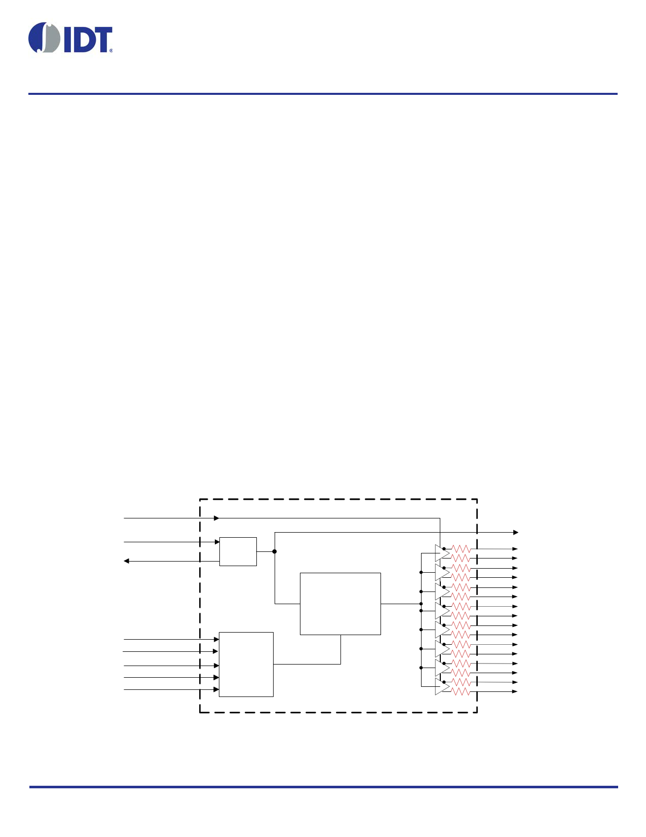
Functional Block Diagram
Features/Benefits
• Direct connection to 100ohm transmission lines; saves 32
resistors compared to standard PCIe devices
• 50mW typical power consumption; reduced thermal
concerns
• Outputs can optionally be supplied from any voltage
between 1.05 and 1.5V; maximum power savings
• OE# pins; support DIF power management
• Programmable Slew rate for each output; allows tuning for
various line length
• Programmable output amplitude; allows tuning for various
application environments
• DIF outputs blocked until PLL is locked; clean system
start-up
• Selectable 0%, -0.25% or -0.5% spread on DIF outputs;
reduces EM
• External 25MHz crystal; supports tight ppm with 0 ppm
synthesis error
• Configuration can be accomplished with strapping pins;
SMBus interface not required for device control
• Selectable SMBus addresses; multiple devices can easily
share an SMBus segment
• 3.3V tolerant SMBus interface works with legacy controllers
• Space saving 48-pin 6x6 mm VFQFPN; minimal board
space
vOE(7:0)#
XIN/CLKIN_25
X2
OSC
vSADR
vSS_EN_tri
^CKPWRGD_PD#
SDATA_3.3
SCLK_3.3
CONTROL
LOGIC
SS Capable PLL
REF1.5
DIF7
DIF6
DIF5
DIF4
DIF3
DIF2
DIF1
DIF0
9FGU0841 OCTOBER 18, 2016
1 ©2016 Integrated Device Technology, Inc.
1 page 
Test Loads
Low-Power HCSL Differential Output Test Load
5 inches
Rs
Zo=100ohm
Rs
Device
REF Output Test Load
Device
Zo = 50 ohms
33
5pF
2pF 2pF
Alternate Terminations
Driving LVDS
Rs
Device
Rs
Cc
Cc
3.3V
R7a
Zo
R8a
R7b
R8b
LVDS Clock
input
Driving LVDS inputs
Value
Receiver has Receiver does not
Component
termination have termination Note
R7a, R7b
10K ohm
140 ohm
R8a, R8b
5.6K ohm
75 ohm
Cc
0.1 uF
0.1 uF
Vcm
1.2 volts
1.2 volts
9FGU0841 DATASHEET
OCTOBER 18, 2016
5 8-OUTPUT 1.5V PCIE GEN1-2-3 CLOCK GENERATOR W/ZO=100OHMS
5 Page 
9FGU0841 DATASHEET
SMBus Table: Output Enable Register 1
Byte 0
Name
Control Function
Type
0
Bit 7
DIF OE7
Output Enable
RW Low/Low
Bit 6
DIF OE6
Output Enable
RW Low/Low
Bit 5
DIF OE5
Output Enable
RW Low/Low
Bit 4
DIF OE4
Output Enable
RW Low/Low
Bit 3
DIF OE3
Output Enable
RW Low/Low
Bit 2
DIF OE2
Output Enable
RW Low/Low
Bit 1
DIF OE1
Output Enable
RW Low/Low
Bit 0
DIF OE0
Output Enable
RW Low/Low
1. A low on these bits will overide the OE# pin and force the differential output Low/Low
1
Enabled
Enabled
Enabled
Enabled
Enabled
Enabled
Enabled
Enabled
Default
1
1
1
1
1
1
1
1
SMBus Table: SS Readback and Control Register
Byte 1
Name
Control Function
Bit 7
Bit 6
SSENRB1
SSENRB1
SS Enable Readback Bit1
SS Enable Readback Bit0
Bit 5
SSEN_SWCNTRL
Enable SW control of SS
Bit 4
SSENSW1
SS Enable Software Ctl Bit1
Bit 3
SSENSW0
SS Enable Software Ctl Bit0
Bit 2
Reserved
Bit 1
Bit 0
AMPLITUDE 1
AMPLITUDE 0
Controls Output Amplitude
1. B1[5] must be set to a 1 for these bits to have any effect on the part.
Type
0
1 Default
R 00' for SS_EN_tri = 0, '01' for SS_EN_tri Latch
R = 'M', '11 for SS_EN_tri = '1' Latch
RW
Values in B1[7:6] Values in B1[4:3]
control SS amount control SS amount.
0
RW1
RW1
RW
RW
00' = SS Off, '01' = -0.25% SS,
'10' = Reserved, '11'= -0.5% SS
00 = 0.55V
10= 0.7V
01 = 0.65V
11 = 0.8V
0
0
1
1
0
SMBus Table: DIF Slew Rate Control Register
Byte 2
Name
Control Function
Bit 7
Bit 6
Bit 5
Bit 4
Bit 3
Bit 2
Bit 1
Bit 0
SLEWRATESEL DIF7
SLEWRATESEL DIF6
SLEWRATESEL DIF5
SLEWRATESEL DIF4
SLEWRATESEL DIF3
SLEWRATESEL DIF2
SLEWRATESEL DIF1
SLEWRATESEL DIF0
Adjust Slew Rate of DIF7
Adjust Slew Rate of DIF6
Adjust Slew Rate of DIF5
Adjust Slew Rate of DIF4
Adjust Slew Rate of DIF3
Adjust Slew Rate of DIF2
Adjust Slew Rate of DIF1
Adjust Slew Rate of DIF0
Type
RW
RW
RW
RW
RW
RW
RW
RW
0
Slow Setting
Slow Setting
Slow Setting
Slow Setting
Slow Setting
Slow Setting
Slow Setting
Slow Setting
1
Fast Setting
Fast Setting
Fast Setting
Fast Setting
Fast Setting
Fast Setting
Fast Setting
Fast Setting
Default
1
1
1
1
1
1
1
1
SMBus Table: Nominal Vhigh Amplitude Control/ REF Control Register
Byte 3
Bit 7
Bit 6
Bit 5
Name
REF
REF Power Down Function
Control Function
Slew Rate Control
Wake-on-Lan Enable for REF
Type
0
1
RW 00 = Slowest
01 = Slow
RW 10 = Fast
11 = Faster
RW
REF does not run in REF runs in Power
Power Down
Down
Bit 4
Bit 3
Bit 2
Bit 1
Bit 0
REF OE
REF Output Enable
Reserved
Reserved
Reserved
Reserved
RW
Low
Enabled
Default
0
1
0
1
1
1
1
1
Byte 4 is Reserved
OCTOBER 18, 2016
11 8-OUTPUT 1.5V PCIE GEN1-2-3 CLOCK GENERATOR W/ZO=100OHMS
11 Page | ||
| Páginas | Total 16 Páginas | |
| PDF Descargar | [ Datasheet 9FGU0841.PDF ] | |
Hoja de datos destacado
| Número de pieza | Descripción | Fabricantes |
| 9FGU0841 | 8-output 1.5V PCIe Gen1-2-3 Clock Generator | IDT |
| Número de pieza | Descripción | Fabricantes |
| SLA6805M | High Voltage 3 phase Motor Driver IC. |
Sanken |
| SDC1742 | 12- and 14-Bit Hybrid Synchro / Resolver-to-Digital Converters. |
Analog Devices |
|
DataSheet.es es una pagina web que funciona como un repositorio de manuales o hoja de datos de muchos de los productos más populares, |
| DataSheet.es | 2020 | Privacy Policy | Contacto | Buscar |