|
|
PDF 8T73S208A-01 Data sheet ( Hoja de datos )
| Número de pieza | 8T73S208A-01 | |
| Descripción | LVPECL Clock Divider and Buffer | |
| Fabricantes | IDT | |
| Logotipo |  |
|
Hay una vista previa y un enlace de descarga de 8T73S208A-01 (archivo pdf) en la parte inferior de esta página. Total 24 Páginas | ||
|
No Preview Available !
2.5V, 3.3V Differential LVPECL Clock
Divider and Buffer
REFER TO PCN# N1605-01, Effective Date August 18, 2016
FOR NEW DESIGNS USE PART NUMBER: 8T73S208B-01NLGI
8T73S208A-01
DATA SHEET
General Description
The 8T73S208A-01 is a high-performance differential LVPECL clock
divider and fanout buffer. The device is designed for the frequency
division and signal fanout of high-frequency, low phase-noise clocks.
The 8T73S208A-01 is characterized to operate from a 2.5V and 3.3V
power supply. Guaranteed output-to-output and part-to-part skew
characteristics make the 8T73S208A-01 ideal for those clock
distribution applications demanding well-defined performance and
repeatability. The integrated input termination resistors make
interfacing to the reference source easy and reduce passive
component count. Each output can be individually enabled or
disabled in the high-impedance state controlled by a I2C register. On
power-up, all outputs are disabled.
Features
• One differential input reference clock
• Differential pair can accept the following differential input
levels: LVDS, LVPECL, CML
• Integrated input termination resistors
• Eight LVPECL outputs
• Selectable clock frequency division of ÷1, ÷2, ÷4 and ÷8
• Maximum input clock frequency: 1GHz
• LVCMOS interface levels for the control inputs
• Individual output enable/disabled by I2C interface
• Power-up state: all outputs disabled
• Output skew: 60ps (maximum)
• Output rise/fall times: 350ps (maximum)
• Low additive phase jitter, RMS: 182fs (typical)
• Full 2.5V and 3.3V supply voltages
• Lead-free (RoHS 6) 32-Lead VFQFN packaging
• -40°C to 85°C ambient operating temperature
8T73S208A-01 REVISION 2 05/20/16
1 ©2016 Integrated Device Technology, Inc.
1 page 
8T73S208A-01 DATA SHEET
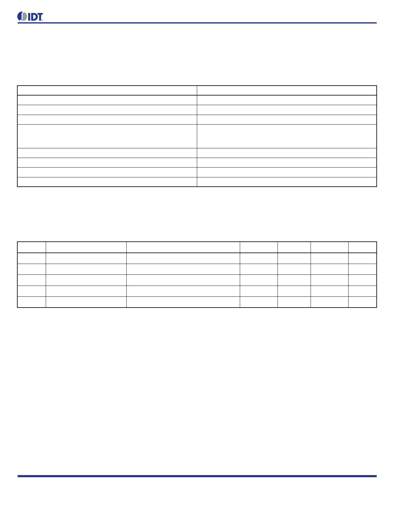
Absolute Maximum Ratings
NOTE: Stresses beyond those listed under Absolute Maximum Ratings may cause permanent damage to the device. These ratings are stress
specifications only. Functional operation of the product at these conditions or any conditions beyond those listed in the DC Characteristics or
AC Characteristics is not implied. Exposure to absolute maximum rating conditions for extended periods may affect product reliability.
Item
Supply Voltage, VCC
Inputs, VI
Input Termination Current, IVT
Outputs, IO (LVPECL)
Continuous Current
Surge Current
Storage Temperature, TSTG
Maximum Junction Temperature, TJMAX
ESD - Human Body Model1
ESD - Charged Device Model
Rating
4.6V
-0.5V to VCC + 0.5V
±35mA
50mA
100mA
-65C to 150C
125°C
2000V
500V
NOTE 1:According to JEDEC/JS-001-2012/JESD22-C101E.
DC Electrical Characteristics
Table 4A. Power Supply DC Characteristics, VCC = VCCO = 2.5V ± 5% or 3.3V ± 5%, VEE = 0V, TA = -40°C to 85°C
Symbol Parameter
Test Conditions
Minimum Typical Maximum Units
VCC
VCC
VCCO
VCCO
IEE
Power Supply Voltage
Power Supply Voltage
Output Supply Voltage
Output Supply Voltage
Power Supply Current
2.375
3.135
2.375
3.135
2.5V
3.3V
2.5V
3.3V
88
2.625
3.465
2.625
3.465
95
V
V
V
V
mA
REVISION 2 05/20/16
5 2.5V, 3.3V DIFFERENTIAL LVPECL CLOCK DIVIDER AND BUFFER
5 Page 
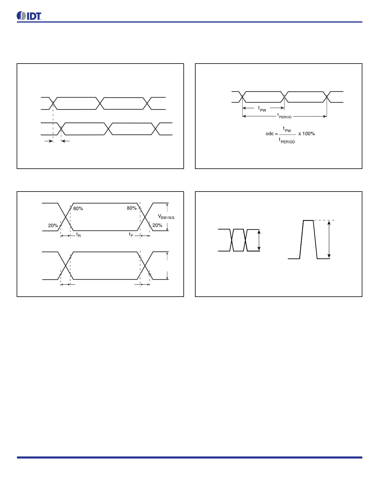
Parameter Measurement Information, continued
8T73S208A-01 DATA SHEET
Part 1
nQx
Qx
Part 2
nQy
Qy
t sk(pp)
Part-to-Part Skew
nQ[0:7]
Q[0:7]
nQ[0:7]
10%
Q[0:7]
90%
tR
Output Rise/Fall Times
nQ[0:7]
Q[0:7]
Output Duty Cycle/Pulse Width/Period
90%
tF
VSW I N G
10%
nIN
VIN
IN
Differential Voltage Swing = 2 x Single-ended VIN
VDIFF_IN
Single-Ended & Differential Input Voltage Swing
REVISION 2 05/20/16
11 2.5V, 3.3V DIFFERENTIAL LVPECL CLOCK DIVIDER AND BUFFER
11 Page | ||
| Páginas | Total 24 Páginas | |
| PDF Descargar | [ Datasheet 8T73S208A-01.PDF ] | |
Hoja de datos destacado
| Número de pieza | Descripción | Fabricantes |
| 8T73S208A-01 | LVPECL Clock Divider and Buffer | IDT |
| Número de pieza | Descripción | Fabricantes |
| SLA6805M | High Voltage 3 phase Motor Driver IC. |
Sanken |
| SDC1742 | 12- and 14-Bit Hybrid Synchro / Resolver-to-Digital Converters. |
Analog Devices |
|
DataSheet.es es una pagina web que funciona como un repositorio de manuales o hoja de datos de muchos de los productos más populares, |
| DataSheet.es | 2020 | Privacy Policy | Contacto | Buscar |
