|
|
|
PDF 8S89833 Data sheet ( Hoja de datos )
| Número de pieza | 8S89833 | |
| Descripción | 1-To-4 Differential-To-LVDS Fanout Buffer w/Internal Termination | |
| Fabricantes | IDT | |
| Logotipo | ||
Hay una vista previa y un enlace de descarga de 8S89833 (archivo pdf) en la parte inferior de esta página. Total 17 Páginas | ||
|
No Preview Available !
Low Skew, 1-To-4 Differential-To-LVDS
Fanout Buffer w/Internal Termination
8S89833
Data Sheet
General Description
The 8S89833 is a high speed 1-to-4 Differential-to-LVDS Fanout
Buffer with Internal Termination. The 8S89833 is optimized for high
speed and very low output skew, making it suitable for use in
demanding applications such as SONET, 1 Gigabit and 10 Gigabit
Ethernet, and Fibre Channel. The internally terminated differential
input and VREF_AC pin allow other differential signal families such as
LVPECL, LVDS, and CML to be easily interfaced to the input with
minimal use of external components. The device also has an output
enable pin which may be useful for system test and debug purposes.
The 8S89833 is packaged in a small 3mm x 3mm 16-pin VFQFN
package which makes it ideal for use in space-constrained
applications.
Features
• Four differential LVDS outputs
• IN, nIN input pair can accept the following differential input levels:
LVPECL, LVDS, CML
• Output frequency: 2GHz
• Cycle-to-cycle jitter, RMS: 3.5ps (maximum)
• Additive phase jitter, RMS: 0.03ps (typical)
• Output skew: 30ps (maximum)
• Part-to-part skew: 200ps (maximum)
• Propagation Delay: 600ps (maximum)
• Full 3.3V supply mode
• -40°C to 85°C ambient operating temperature
• Available in lead-free (RoHS 6) package
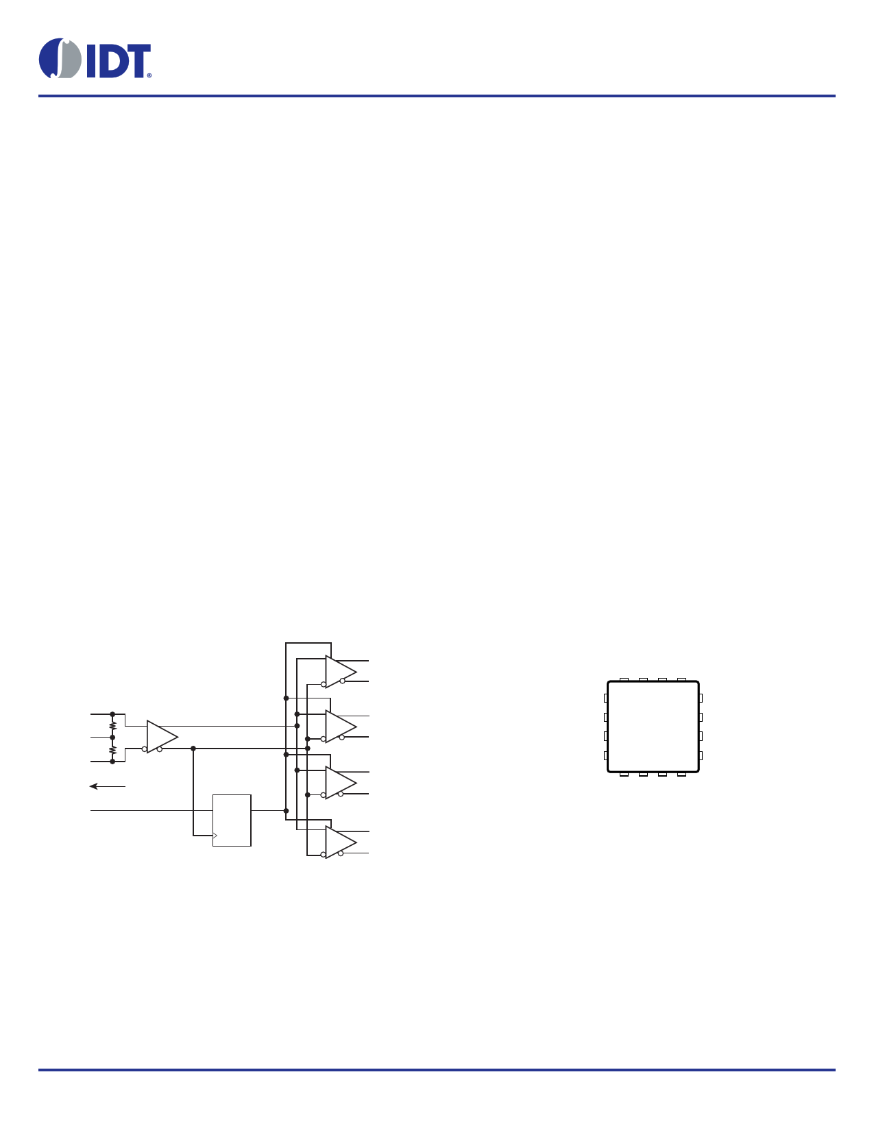
Block Diagram
IN
50Ω
VT
50Ω
nIN
VREF_AC
EN Pullup
DQ
Q0
nQ0
Q1
nQ1
Q2
nQ2
Q3
nQ3
Pin Assignment
16 15 14 13
Q0 1
12 IN
nQ0 2
11 VT
Q1 3
10 VREF_AC
nQ1 4
9 nIN
5 6 78
8S89833
16-Lead VFQFN
3mm x 3mm x 0.925mm package body
K Package
Top View
©2016 Integrated Device Technology, Inc
1
Revision B August 24, 2016
1 page 
8S89833 Data Sheet
Table 4C. Differential DC Characteristics, VDD = 3.3V ± 0.3V, TA = -40°C to 85°C
Symbol Parameter
Test Conditions
Minimum
RDIFF_IN
RIN
VIH
VIL
VIN
VDIFF_IN
VREF_AC
IIN
Differential Input Resistance (IN, nIN)
Input Resistance
Input High Voltage
(IN, nIN)
Input Low Voltage
(IN, nIN)
Input Voltage Swing
Differential Input Voltage Swing
Bias Voltage
Input Current; NOTE 1
IN-to-VT
IN-to-VT
80
40
1.2
0
0.15
0.3
VDD – 1.44
NOTE 1: Guaranteed by design.
Typical
100
50
VDD – 1.38
Maximum
120
60
VDD
VIH – 0.15
1.2
VDD – 1.32
35
Units
V
V
V
V
V
mA
Table 4D. LVDS DC Characteristics, VDD = 3.3V ± 0.3V, TA = -40°C to 85°C
Symbol Parameter
Test Conditions
VOD
VOD
VOS
VOS
Differential Output Voltage
VOD Magnitude Change
Offset Voltage
VOS Magnitude Change
Minimum
247
1.2
Typical
1.4
Maximum
454
50
1.6
50
Units
mV
V
V
mV
©2016 Integrated Device Technology, Inc
5
Revision B August 24, 2016
5 Page 
8S89833 Data Sheet
VFQFN EPAD Thermal Release Path
In order to maximize both the removal of heat from the package and
the electrical performance, a land pattern must be incorporated on
the Printed Circuit Board (PCB) within the footprint of the package
corresponding to the exposed metal pad or exposed heat slug on the
package, as shown in Figure 3. The solderable area on the PCB, as
defined by the solder mask, should be at least the same size/shape
as the exposed pad/slug area on the package to maximize the
thermal/electrical performance. Sufficient clearance should be
designed on the PCB between the outer edges of the land pattern
and the inner edges of pad pattern for the leads to avoid any shorts.
While the land pattern on the PCB provides a means of heat transfer
and electrical grounding from the package to the board through a
solder joint, thermal vias are necessary to effectively conduct from
the surface of the PCB to the ground plane(s). The land pattern must
be connected to ground through these vias. The vias act as “heat
pipes”. The number of vias (i.e. “heat pipes”) are application specific
and dependent upon the package power dissipation as well as
electrical conductivity requirements. Thus, thermal and electrical
analysis and/or testing are recommended to determine the minimum
number needed. Maximum thermal and electrical performance is
achieved when an array of vias is incorporated in the land pattern. It
is recommended to use as many vias connected to ground as
possible. It is also recommended that the via diameter should be 12
to 13mils (0.30 to 0.33mm) with 1oz copper via barrel plating. This is
desirable to avoid any solder wicking inside the via during the
soldering process which may result in voids in solder between the
exposed pad/slug and the thermal land. Precautions should be taken
to eliminate any solder voids between the exposed heat slug and the
land pattern. Note: These recommendations are to be used as a
guideline only. For further information, please refer to the Application
Note on the Surface Mount Assembly of Amkor’s
Thermally/Electrically Enhance Leadframe Base Package, Amkor
Technology.
PIN SOLDER
EXPOSED HEAT SLUG
SOLDER
PIN
PIN PAD
GROUND PLANE
THERMAL VIA
LAND PATTERN
(GROUND PAD)
PIN PAD
Figure 3. P.C. Assembly for Exposed Pad Thermal Release Path – Side View (drawing not to scale)
LVDS Driver Termination
A general LVDS interface is shown in Figure 4. Standard termination
for LVDS type output structure requires both a 100 parallel resistor
at the receiver and a 100 differential transmission line environment.
In order to avoid any transmission line reflection issues, the 100
resistor must be placed as close to the receiver as possible. IDT
offers a full line of LVDS compliant devices with two types of output
structures: current source and voltage source. The standard
termination schematic as shown in Figure X can be used with either
type of output structure. If using a non-standard termination, it is
recommended to contact IDT and confirm if the output is a current
source or a voltage source type structure. In addition, since these
outputs are LVDS compatible, the amplitude and common mode
input range of the input receivers should be verified for compatibility
with the output.
LVDS Driver
100Ω
+
LVDS
Receiver
–
100Ω Differential Transmission Line
Figure 4. Typical LVDS Driver Termination
©2016 Integrated Device Technology, Inc
11
Revision B August 24, 2016
11 Page | ||
| Páginas | Total 17 Páginas | |
| PDF Descargar | [ Datasheet 8S89833.PDF ] | |
Hoja de datos destacado
| Número de pieza | Descripción | Fabricantes |
| 8S89831I | Differential LVPECL-To-LVPECL/ECL Fanout Buffer | IDT |
| 8S89832I | 1-to-4 Differential-to-LVDS Fanout Buffer | IDT |
| 8S89833 | 1-To-4 Differential-To-LVDS Fanout Buffer w/Internal Termination | IDT |
| 8S89834I | 2-to-4 LVCMOS/LVTTL-toLVPECL/ECL Clock Multiplexer | IDT |
| Número de pieza | Descripción | Fabricantes |
| SLA6805M | High Voltage 3 phase Motor Driver IC. |
Sanken |
| SDC1742 | 12- and 14-Bit Hybrid Synchro / Resolver-to-Digital Converters. |
Analog Devices |
|
DataSheet.es es una pagina web que funciona como un repositorio de manuales o hoja de datos de muchos de los productos más populares, |
| DataSheet.es | 2020 | Privacy Policy | Contacto | Buscar |