|
|
|
PDF ADP7158 Data sheet ( Hoja de datos )
| Número de pieza | ADP7158 | |
| Descripción | RF Linear Regulator | |
| Fabricantes | Analog Devices | |
| Logotipo | ||
Hay una vista previa y un enlace de descarga de ADP7158 (archivo pdf) en la parte inferior de esta página. Total 23 Páginas | ||
|
No Preview Available !
Data Sheet
2 A, Ultralow Noise,
High PSRR, RF Linear Regulator
ADP7158
FEATURES
Input voltage range: 2.3 V to 5.5 V
16 standard voltages between 1.2 V and 3.3 V available
Maximum load current: 2 A
Low noise
0.9 μV rms total integrated noise from 100 Hz to 100 kHz
1.6 μV rms total integrated noise from 10 Hz to 100 kHz
Noise spectral density: 1.7 nV/√Hz from 10 kHz to 1 MHz
Power supply rejection ratio (PSRR)
70 dB from 1 kHz to 100 kHz; 50 dB at 1 MHz, VOUT = 3.3 V,
VIN = 4.0 V
Dropout voltage: 200 mV typical at IOUT = 2 A, VOUT = 3.3 V
Initial accuracy: ±0.6% at ILOAD = 10 mA
Accuracy over line, load, and temperature: ±1.5%
Quiescent current: IGND = 4.0 mA at no load, 9.0 mA at 2 A
Low shutdown current: 0.2 μA
Stable with a 10 μF ceramic output capacitor
10-lead, 3 mm × 3 mm LFCSP and 8-lead SOIC packages
Precision enable
Supported by ADIsimPower tool
APPLICATIONS
Regulation to noise sensitive applications: phase-locked
loops (PLLs), voltage controlled oscillators (VCOs), and
PLLs with integrated VCOs
Communications and infrastructure
Backhaul and microwave links
GENERAL DESCRIPTION
The ADP7158 is a linear regulator that operates from 2.3 V to
5.5 V and provides up to 2 A of output current. Using an advanced
proprietary architecture, it provides high power supply rejection
and ultralow noise, achieving excellent line and load transient
response with only a 10 μF ceramic output capacitor.
There are 16 standard output voltages for the ADP7158. The
following voltages are available from stock: 1.2 V, 1.8 V, 2.0 V,
2.5 V, 2.8 V, 3.0 V and 3.3 V. Additional voltages available by
special order are 1.3 V, 1.5 V, 1.6 V, 2.2 V, 2.6 V, 2.7 V, 2.9 V,
3.1V and 3.2 V.
The ADP7158 regulator typical output noise is 0.9 μV rms
from 100 Hz to 100 kHz and 1.7 nV/√Hz for noise spectral
density from 10 kHz to 1 MHz. The ADP7158 is available in a
10-lead, 3 mm × 3 mm LFCSP and 8-lead SOIC packages,
making it not only a very compact solution, but also providing
excellent thermal performance for applications requiring up to
2 A of output current in a small, low profile footprint.
TYPICAL APPLICATION CIRCUIT
VIN = 3.8V
CIN
10µF
ON
OFF
CBYP
1µF
ADP7158
VIN VOUT
VOUT_SENSE
EN
BYP
REF
REF_SENSE
VOUT = 3.3V
COUT
10µF
CREF
1µF
CREG
1µF
VREG
GND (EPAD)
Figure 1.
Table 1. Related Devices
Model
Input
Voltage
ADP7159 2.3 V to 5.5 V
ADP7156,
ADP7157
ADM7150,
ADM7151
ADM7154,
ADM7155
ADM7160
2.3 V to 5.5 V
4.5 V to 16 V
2.3 V to 5.5 V
2.2 V to 5.5 V
Output
Current
2A
Fixed/
Adj1
Adj
1.2 A
800 mA
600 mA
200 mA
Fixed/
Adj
Fixed/
Adj
Fixed/
Adj
Fixed
Package
10-lead LFCSP/
8-lead SOIC
10-lead LFCSP/
8-lead SOIC
8-lead LFCSP/
8-lead SOIC
8-lead LFCSP/
8-lead SOIC
6-lead LFCSP/
5-lead TSOT
1 Adj means adjustable.
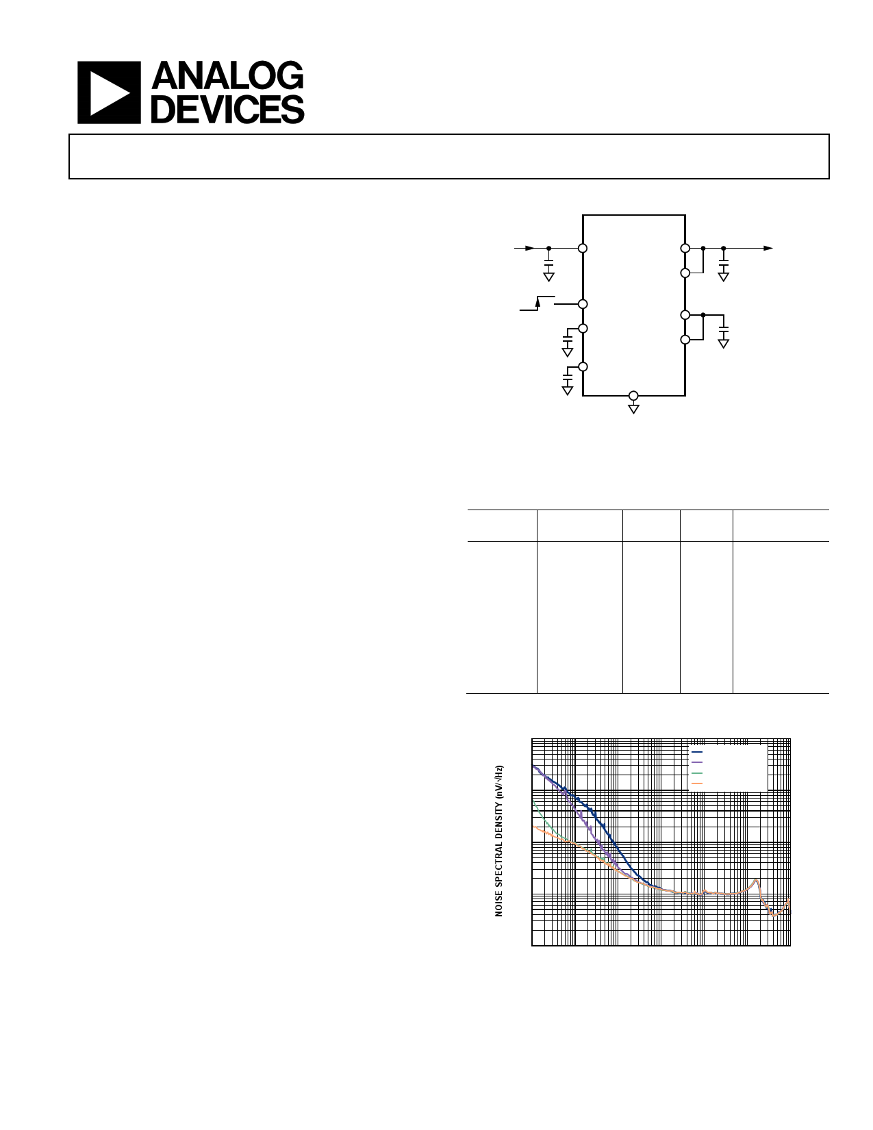
1k
CBYP = 1µF
CBYP = 10µF
CBYP = 100µF
100 CBYP = 1000µF
10
1
0.1
10 100 1k 10k 100k 1M 10M
FREQUENCY (Hz)
Figure 2. Noise Spectral Density at Various Values of CBYP, VOUT = 3.3 V
Rev. A
Document Feedback
Information furnished by Analog Devices is believed to be accurate and reliable. However, no
responsibility is assumed by Analog Devices for its use, nor for any infringements of patents or other
rights of third parties that may result from its use. Specifications subject to change without notice. No
license is granted by implication or otherwise under any patent or patent rights of Analog Devices.
Trademarksandregisteredtrademarksarethepropertyoftheirrespectiveowners.
One Technology Way, P.O. Box 9106, Norwood, MA 02062-9106, U.S.A.
Tel: 781.329.4700
©2016 Analog Devices, Inc. All rights reserved.
Technical Support
www.analog.com
1 page 
ADP7158
Data Sheet
Parameter
VREG UVLO THRESHOLDS7
Rising
Falling
Hysteresis
EN INPUT PRECISION
EN Input
Logic High
Logic Low
Logic Hysteresis
LEAKAGE CURRENT
REF_SENSE
EN
Symbol
Test Conditions/Comments
VREGUVLORISE
VREGUVLOFALL
VREGUVLOHYS
2.3 V ≤ VIN ≤ 5.5 V
VEN_HIGH
VEN_LOW
VEN_HYS
IREF_SENSE_LKG
IEN_LKG
EN = VIN or GND
Min Typ Max Unit
1.94 V
1.60 V
185 mV
1.13 1.22 1.31 V
1.05 1.13 1.22 V
90 mV
10
0.01 1
nA
μA
1 Guaranteed by characterization but not production tested.
2 The ADP7158 is available in 16 standard voltages between 1.2 V and 3.3 V, including 1.2 V, 1.3 V, 1.5 V, 1.6 V, 1.8 V, 2.0 V, 2.2 V, 2.5 V, 2.6 V, 2.7 V, 2.8 V, 2.9 V, 3.0 V, 3.1 V,
3.2 V, and 3.3 V.
3 Based on an endpoint calculation using 10 mA and 2 A loads.
4 Current-limit threshold is defined as the current at which the output voltage drops to 90% of the specified typical value. For example, the current limit for a 3.0 V
output voltage is defined as the current that causes the output voltage to drop to 90% of 3.0 V, or 2.7 V.
5 Dropout voltage is defined as the input to output voltage differential when the input voltage is set to the nominal output voltage. Dropout voltage applies only for
output voltages greater than 2.3 V.
6 Start-up time is defined as the time between the rising edge of VEN to VOUT, VREG, or VREF being at 90% of its nominal value.
7 The output voltage is disabled until the VREG UVLO rise threshold is crossed. The VREG output is disabled until the input voltage UVLO rising threshold is crossed.
INPUT AND OUTPUT CAPACITORS, RECOMMENDED SPECIFICATIONS
Table 3.
Parameter
MINIMUM CAPACITANCE
Input1
Regulator
Output1
Bypass
Reference
CAPACITOR EFFECTIVE SERIES RESISTANCE (ESR)
COUT, CIN
CREG, CREF
CBYP
Symbol
CIN
CREG
COUT
CBYP
CREF
RESR
RESR
RESR
Test Conditions/Comments
TA = −40°C to +125°C
TA = −40°C to +125°C
Min Typ Max Unit
10.0 μF
1.0 μF
10.0 μF
1.0 μF
1.0 μF
0.001
0.001
0.001
0.1 Ω
0.2 Ω
2.0 Ω
1 The minimum input and output capacitance must be greater than 7.0 μF over the full range of operating conditions. The full range of operating conditions in the
application must be considered during device selection to ensure that the minimum capacitance specification is met. X7R and X5R type capacitors are recommended;
Y5V and Z5U capacitors are not recommended for use with any low dropout regulator.
Rev. A | Page 4 of 22
5 Page 
ADP7158
0
10Hz
–10 100Hz
1kHz
–20
10kHz
100kHz
–30
1MHz
10MHz
–40
–50
–60
–70
–80
–90
–100
0.5
0.6 0.7 0.8
HEADROOM VOLTAGE (V)
0.9
Figure 23. Power Supply Rejection Ratio (PSRR) vs. Headroom Voltage
at Various Frequencies, VOUT = 3.3 V, 2 A Load
0
–10
ILOAD = 10mA
ILOAD = 100mA
–20
ILOAD = 600mA
ILOAD = 1200mA
–30 ILOAD = 2000mA
–40
–50
–60
–70
–80
–90
–100
1
10 100 1k 10k 100k 1M 10M
FREQUENCY (Hz)
Figure 24. Power Supply Rejection Ratio (PSRR) vs. Frequency
at Various Loads, VOUT = 1.8 V, VIN = 2.6 V
0
–10
–20
–30
900mV
800mV
700mV
–40 600mV
500mV
–50
–60
–70
–80
–90
–100
1
10 100 1k 10k 100k 1M 10M
FREQUENCY (Hz)
Figure 25. Power Supply Rejection Ratio (PSRR) vs. Frequency
at Various Headroom Voltages, VOUT = 1.8 V, 2 A Load
Data Sheet
0 10Hz
–10
100Hz
1kHz
10kHz
–20 100kHz
1MHz
–30 10MHz
–40
–50
–60
–70
–80
–90
–100
0.5
0.6 0.7 0.8
HEADROOM VOLTAGE (V)
0.9
Figure 26. Power Supply Rejection Ratio (PSRR) vs. Headroom Voltage
at Various Frequencies, VOUT = 1.8 V, 2 A Load
0
–10
–20
CBYP = 1µF
CBYP = 10µF
–30
CBYP = 100µF
CBYP = 1000µF
–40
–50
–60
–70
–80
–90
–100
1
10 100 1k 10k 100k 1M 10M
FREQUENCY (Hz)
Figure 27. Power Supply Rejection Ratio (PSRR) vs. Frequency
at Various CBYP Values, VOUT = 3.3 V, VIN = 4.0 V, 2 A Load
2.0
1.8
10Hz TO 100kHz
1.6
1.4
1.2
1.0 100Hz TO 100kHz
0.8
0.6
0.4
0.2
0
10m
100m
1
LOAD CURRENT (A)
Figure 28. RMS Output Noise vs. Load Current
10
Rev. A | Page 10 of 22
11 Page | ||
| Páginas | Total 23 Páginas | |
| PDF Descargar | [ Datasheet ADP7158.PDF ] | |
Hoja de datos destacado
| Número de pieza | Descripción | Fabricantes |
| ADP7156 | RF Linear Regulator | Analog Devices |
| ADP7157 | RF Linear Regulator | Analog Devices |
| ADP7158 | RF Linear Regulator | Analog Devices |
| ADP7159 | RF Linear Regulator | Analog Devices |
| Número de pieza | Descripción | Fabricantes |
| SLA6805M | High Voltage 3 phase Motor Driver IC. |
Sanken |
| SDC1742 | 12- and 14-Bit Hybrid Synchro / Resolver-to-Digital Converters. |
Analog Devices |
|
DataSheet.es es una pagina web que funciona como un repositorio de manuales o hoja de datos de muchos de los productos más populares, |
| DataSheet.es | 2020 | Privacy Policy | Contacto | Buscar |