|
|
|
PDF NJVMJB42CT4G Data sheet ( Hoja de datos )
| Número de pieza | NJVMJB42CT4G | |
| Descripción | Complementary Silicon Plastic Power Transistors | |
| Fabricantes | ON Semiconductor | |
| Logotipo | ||
Hay una vista previa y un enlace de descarga de NJVMJB42CT4G (archivo pdf) en la parte inferior de esta página. Total 6 Páginas | ||
|
No Preview Available !
MJB41C,
NJVMJB41CT4G (NPN),
MJB42C,
NJVMJB42CT4G (PNP)
Complementary Silicon
Plastic Power Transistors
D2PAK for Surface Mount
Features
• Lead Formed for Surface Mount Applications in Plastic Sleeves
(No Suffix)
• Electrically the Same as TIP41 and T1P42 Series
• NJV Prefix for Automotive and Other Applications Requiring
Unique Site and Control Change Requirements; AEC−Q101
Qualified and PPAP Capable
• Pb−Free Packages are Available
MAXIMUM RATINGS
Rating
Symbol
Value
Unit
Collector−Emitter Voltage
ÎÎÎÎÎÎÎÎÎÎÎÎÎÎÎÎÎÎÎCollector−Base Voltage
ÎÎÎÎÎÎÎÎÎÎÎÎÎÎÎÎÎÎÎEmitter−Base Voltage
ÎÎÎÎÎÎÎÎÎÎÎÎÎÎÎÎÎÎÎCollector Current − Continuous
ÎÎÎÎÎÎÎÎÎÎÎÎÎÎÎÎÎÎÎ− Peak
VCEO 100 Vdc
VCB 100 Vdc
VEB 5.0 Vdc
IC 6.0 Adc
10
ÎÎÎÎÎÎÎÎÎÎÎÎÎÎÎÎÎÎÎBase Current
ÎÎÎÎÎÎÎÎÎÎÎÎÎÎÎÎÎÎÎTotal Power Dissipation
ÎÎÎÎÎÎÎÎÎÎÎÎÎÎÎÎÎÎÎ@ TC = 25_C
Derate above 25_C
IB 2.0 Adc
PD
65 W
0.52 W/_C
ÎÎÎÎÎÎÎÎÎÎÎÎÎÎÎÎÎÎÎTotal Power Dissipation
ÎÎÎÎÎÎÎÎÎÎÎÎÎÎÎÎÎÎÎ@ TA = 25_C
Derate above 25_C
PD
2.0 W
0.016
W/_C
ÎÎÎÎÎÎÎÎÎÎÎÎÎÎÎÎÎÎÎUnclamped Inductive Load Energy (Note 1)
E
62.5 mJ
ÎÎÎÎÎÎÎÎÎÎÎÎÎÎÎÎÎÎÎOperating and Storage Junction
ÎÎÎÎÎÎÎÎÎÎÎÎÎÎÎÎÎÎÎTemperature Range
TJ, Tstg −65 to +150 _C
ÎÎÎÎÎÎÎÎÎÎÎÎÎÎÎÎÎÎÎTHERMAL CHARACTERISTICS
ÎÎÎÎÎÎÎÎÎÎÎÎÎÎÎÎÎÎÎCharacteristic
Symbol
Max
Unit
ÎÎÎÎÎÎÎÎÎÎÎÎÎÎÎÎÎÎÎThermal Resistance, Junction−to−Case
ÎÎÎÎÎÎÎÎÎÎÎÎÎÎÎÎÎÎÎThermal Resistance,
ÎÎÎÎÎÎÎÎÎÎÎÎÎÎÎÎÎÎÎJunction−to−Ambient
RqJC
RqJA
1.92 _C/W
62.5 _C/W
ÎÎÎÎÎÎÎÎÎÎÎÎÎÎÎÎÎÎÎThermal Resistance,
Junction−to−Ambient (Note 2)
RqJA
50 _C/W
ÎÎÎÎÎÎÎÎÎÎÎÎÎÎÎÎÎÎÎMaximum Lead Temperature for Soldering
ÎÎÎÎÎÎÎÎÎÎÎÎÎÎÎÎÎÎÎPurposes, 1/8″ from Case for 10 Seconds
TL
260 _C
ÎÎÎÎÎÎÎÎÎÎÎÎÎÎÎÎÎÎÎStresses exceeding Maximum Ratings may damage the device. Maximum
Ratings are stress ratings only. Functional operation above the Recommended
Operating Conditions is not implied. Extended exposure to stresses above the
Recommended Operating Conditions may affect device reliability.
1. IC = 2.5 A, L = 20 mH, P.R.F. = 10 Hz, VCC = 10 V, RBE = 100 W
2. When surface mounted to an FR−4 board using the minimum recommended
pad size.
© Semiconductor Components Industries, LLC, 2013
May, 2013 − Rev. 4
1
http://onsemi.com
COMPLEMENTARY SILICON
POWER TRANSISTORS
6 AMPERES,
100 VOLTS, 65 WATTS
MARKING
DIAGRAM
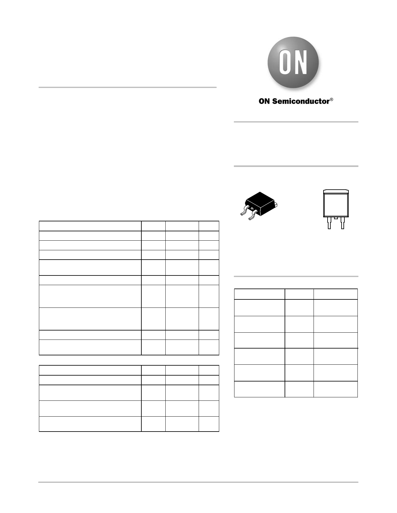
D2PAK
CASE 418B
STYLE 1
J4xCG
AYWW
J4xC
A
Y
WW
G
= Specific Device Code
x = 1 or 2
= Assembly Location
= Year
= Work Week
= Pb−Free Package
ORDERING INFORMATION
Device
Package
Shipping†
MJB41CG
D2PAK
50 Units / Rail
(Pb−Free)
MJB41CT4G
D2PAK
(Pb−Free)
800 / Tape &
Reel
NJVMJB41CT4G
D2PAK
(Pb−Free)
800 / Tape &
Reel
MJB42CG
D2PAK
50 Units / Rail
(Pb−Free)
MJB42CT4G
D2PAK
(Pb−Free)
800 / Tape &
Reel
NJVMJB42CT4G
D2PAK
(Pb−Free)
800 / Tape &
Reel
†For information on tape and reel specifications,
including part orientation and tape sizes, please
refer to our Tape and Reel Packaging Specifications
Brochure, BRD8011/D.
Publication Order Number:
MJB41C/D
1 page 
MJB41C, NJVMJB41CT4G (NPN), MJB42C, NJVMJB42CT4G (PNP)
PACKAGE DIMENSIONS
D2PAK 3
CASE 418B−04
ISSUE K
C
−B−
4
E
V
W
123
S
−T−
SEATING
PLANE
G
K
D 3 PL
0.13 (0.005) M T B M
A
W
J
H
VARIABLE
CONFIGURATION
ZONE
L
M
R
M
N
L
U
M
NOTES:
1. DIMENSIONING AND TOLERANCING
PER ANSI Y14.5M, 1982.
2. CONTROLLING DIMENSION: INCH.
3. 418B−01 THRU 418B−03 OBSOLETE,
NEW STANDARD 418B−04.
INCHES
DIM MIN MAX
A 0.340 0.380
B 0.380 0.405
C 0.160 0.190
D 0.020 0.035
E 0.045 0.055
F 0.310 0.350
G 0.100 BSC
H 0.080 0.110
J 0.018 0.025
K 0.090 0.110
L 0.052 0.072
M 0.280 0.320
N 0.197 REF
P 0.079 REF
R 0.039 REF
S 0.575 0.625
V 0.045 0.055
MILLIMETERS
MIN MAX
8.64 9.65
9.65 10.29
4.06 4.83
0.51 0.89
1.14 1.40
7.87 8.89
2.54 BSC
2.03 2.79
0.46 0.64
2.29 2.79
1.32 1.83
7.11 8.13
5.00 REF
2.00 REF
0.99 REF
14.60 15.88
1.14 1.40
STYLE 1:
PIN 1. BASE
2. COLLECTOR
3. EMITTER
4. COLLECTOR
P
L
F
VIEW W−W
1
FF
VIEW W−W
2
VIEW W−W
3
SOLDERING FOOTPRINT*
10.49
16.155
8.38
2X
1.016
2X
3.504
5.080
PITCH
DIMENSIONS: MILLIMETERS
*For additional information on our Pb−Free strategy and soldering
details, please download the ON Semiconductor Soldering and
Mounting Techniques Reference Manual, SOLDERRM/D.
http://onsemi.com
5
5 Page | ||
| Páginas | Total 6 Páginas | |
| PDF Descargar | [ Datasheet NJVMJB42CT4G.PDF ] | |
Hoja de datos destacado
| Número de pieza | Descripción | Fabricantes |
| NJVMJB42CT4G | Complementary Silicon Plastic Power Transistors | ON Semiconductor |
| Número de pieza | Descripción | Fabricantes |
| SLA6805M | High Voltage 3 phase Motor Driver IC. |
Sanken |
| SDC1742 | 12- and 14-Bit Hybrid Synchro / Resolver-to-Digital Converters. |
Analog Devices |
|
DataSheet.es es una pagina web que funciona como un repositorio de manuales o hoja de datos de muchos de los productos más populares, |
| DataSheet.es | 2020 | Privacy Policy | Contacto | Buscar |