|
|
|
PDF LTC3649 Data sheet ( Hoja de datos )
| Número de pieza | LTC3649 | |
| Descripción | 4A Synchronous Step-Down Regulator | |
| Fabricantes | Linear | |
| Logotipo | ||
Hay una vista previa y un enlace de descarga de LTC3649 (archivo pdf) en la parte inferior de esta página. Total 26 Páginas | ||
|
No Preview Available !
LTC3649
FEATURES
60V, 4A Synchronous
Step-Down Regulator with
Rail-to-Rail Programmable Output
DESCRIPTION
nn Wide VIN Range: 3.1V to 60V
nn Wide VOUT Range: 0V to (VIN – 0.5V)
nn Single Resistor VOUT Programming
nn Integrated 110mΩ Top N-Channel/50mΩ Bottom
N-Channel MOSFETs
nn 95% Efficiency with 12VIN and 5VOUT
nn Regulated IQ: 440µA, Shutdown IQ: 18µA
nn Accurate Current Monitoring (±4%) without Sense
Resistor
nn Accurate Resistor Programmable Frequency
(300kHz to 3MHz) with ±50% Frequency Sync Range
nn Accurate Programmable Output Current
nn Input Voltage Regulation for MPPT Applications
nn ±0.8% Output Voltage Accuracy
nn Peak Current Mode Operation
nn Programmable Wire Drop Compensation
nn Burst Mode® Operation, Forced Continuous Mode
nn Internal Compensation and Programmable Soft-Start
nn Overtemperature Protection
nn Available in Thermally Enhanced 28-Lead (4mm ×
5mm) QFN and TSSOP Packages
APPLICATIONS
nn Industrial Applications
nn Automotive Applications
The LTC®3649 is a high efficiency 60V, 4A synchronous
monolithic step-down regulator. The regulator features
a single resistor programmable output voltage, internal
compensation and high efficiencies over a wide VOUT range.
The step-down regulator operates from an input voltage
range of 3.1V to 60V and provides an adjustable rail-to-rail
output range from (VIN – 0.5V) to ground while delivering
up to 4A of output current. The switching frequency is
also adjusted with an external resistor. A user-selectable
mode input is provided to allow the user to trade off ripple
noise for efficiency at light loads; Burst Mode operation
provides the highest efficiency at light loads, while forced
continuous mode provides low output ripple. The MODE/
SYNC pin can also be used to allow the user to synchronize
the switching frequency to an external clock.
The LTC3649 operates with a peak current mode architec-
ture that allows for fast transient response with inherent
cycle-to-cycle current limit protection. It also features
programmable output current limit, current monitoring
and input voltage regulation.
L, LT, LTC, LTM, Linear Technology, the Linear logo, Burst Mode and OPTI-LOOP are
registered trademarks of Linear Technology Corporation. All other trademarks are the property
of their respective owners. Protected by U.S. Patents, including 5481178, 5705919, 5847554,
6580258.
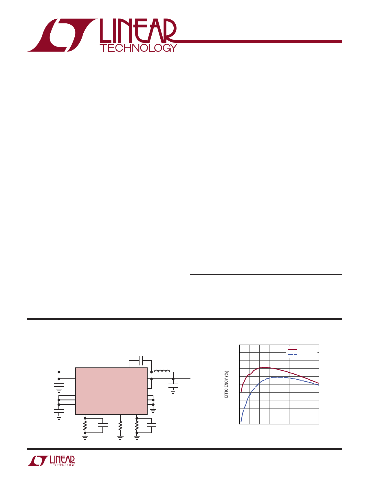
TYPICAL APPLICATION
24V to 5VOUT Burst Mode Operation
0.1µF
VIN
5.5V TO 60V
22µF
VIN
RUN
ITH
VINREG
INTVCC
2.2µF ISET
BOOST SW
VOUT
LTC3649
EXTVCC
MODE/SYNC
SGND
PGND
RT IMON
100k
10nF 200k 10k
fSW = 500kHz
6.8µH
10nF
47µF
×2
VOUT
5V
4A
3649 TA01a
100
98
96
94
92
90
88
86
84
82
80
0
Efficiency with VOUT = 5V
VIN = 12V
VIN = 24V
0.5 1 1.5 2 2.5 3 3.5 4
IOUT (A)
3649 TA01b
For more information www.linear.com/LTC3649
3649fa
1
1 page 
LTC3649
TYPICAL PERFORMANCE CHARACTERISTICS TA = 25°C, unless otherwise noted.
RDS(ON) vs Temperature
200
Transient Response, CCM
Transient Response, Burst Mode
160
MTOP
VOUT
100mV/DIV
120 AC-COUPLED
VOUT
100mV/DIV
AC-COUPLED
80
MBOT
40
0
–55 –35 –15 5 25 45 65 85 105 125
TEMPERATURE (°C)
3649 G07
IL
2A/DIV
20µs/DIV
3649 G08
VIN = 24V, VOUT = 5V
IOUT = 0A TO 4A, L = 2.2µH, fSW = 1MHz
RITH = 4kΩ, CITH = 2.2nF, CITHP = 47pF
FC MODE, COUT = 2× 47µF
IL
2A/DIV
20µs/DIV
3649 G09
VIN = 24V, VOUT = 5V
IOUT = 0.2A TO 4A, L = 2.2µH, fSW = 1MHz
RITH = 4kΩ, CITH = 2.2nF, CITHP = 47pF
BURST MODE, COUT = 2× 47µF
Switching Frequency/Period
vs RT
3.0
3500
2.5
FREQUENCY
2.0
1.5
1.0
0.5
PERIOD
3000
2500
2000
1500
1000
500
00
0 50 100 150 200 250 300 350
RT RESISTOR (kΩ)
3649 G10
Switching Frequency
vs Temperature
1010
Output Regulation with VIN Slew
1005
IL
1A/DIV
1000
VOUT
2V/DIV
995
VIN
50V/DIV
990
985
–55 –35 –15 5 25 45 65 85 105 125
TEMPERATURE (°C)
10ms/DIV
VIN = 12V TO 60V, VOUT = 5V
IOUT = 0A, L = 2.2µH, fSW = 2.25MHz
RITH = 4kΩ, CITH = 2.2nF, CITHP = 47pF
FC MODE, COUT = 2× 47µF
3649 G11
3649 G12
Burst Mode Operation
Continuous Conduction Mode
Operation
Run Rising Threshold
vs Temperature
1.210
IL
1A/DIV
IL
1A/DIV
1.205
1.200
SW
10V/DIV
2µs/DIV
VIN = 24V, VOUT = 5V
IOUT = 100mA, L = 2.2µH, fSW = 1MHz
RITH = 4kΩ, CITH = 2.2nF, CITHP = 47pF
BURST MODE, COUT = 2× 47µF
3649 G13
SW
10V/DIV
500ns/DIV
VIN = 24V, VOUT = 5V
IOUT = 0A, L = 2.2µH, fSW = 1MHz
RITH = 4kΩ, CITH = 2.2nF, CITHP = 47pF
FC MODE, COUT = 2× 47µF
3649 G14
For more information www.linear.com/LTC3649
1.195
1.190
1.185
1.180
–55 –35 –15 5 25 45 65 85 105 125
TEMPERATURE (°C)
3649 G15
3649fa
5
5 Page 
LTC3649
OPERATION
the input to hold the input voltage at the regulated point.
The regulator will continue to perform this operation until
the output capacitor has dissipated so much energy that it
can no longer hold up the input voltage. This momentary
input voltage holdup proves to be a handy tool for certain
applications.
INTVCC Regulator
The LTC3649 has two onboard internal low dropout (LDO)
regulators that power the drivers and internal bias circuitry.
Regardless of which one is in operation, the INTVCC must
be bypassed to GND with a minimum of 2.2µF ceramic
capacitor. Good bypassing is necessary to supply the
high transient current required by the power MOSFET
gate drivers.
The first LDO is powered from VIN, and the INTVCC volt-
age is regulated to 3.3V. The power dissipated across
this LDO would thus equal to (VIN – 3.3) • IINTVCC. For
a typical 1MHz application running in CCM, the current
drawn from INTVCC by the chip is roughly 20mA. Thus,
if the input voltage is high, the power loss and heat rise
due to this LDO is significant.
To combat this issue, a separate LDO exists that is powered
from EXTVCC. As long as the input voltage is above 5V
and the EXTVCC voltage is above 3.2V, this LDO will take
over and regulate the INTVCC voltage to 3.1V. In applica-
tions where the output voltage is programmed to 3.3V or
above, it is recommended that the VOUT (<28V) pin be
directly tied to the EXTVCC pin. Otherwise, if a separate
lower voltage rail exists on board that can supply INTVCC
current, then attaching that supply to EXTVCC will also
suffice provided that a 1µF ceramic bypass capacitor is
placed from the EXTVCC pin to GND physically close to
the chip. Both examples should significantly reduce the
power loss through the LDO.
VIN Undervoltage Programming
LTC3649 offers an accurate RUN threshold to start the
regulator. As a result, a resistor divider from IN to GND
can be placed with the intermediate node fed back to RUN
to set an accurate VIN undervoltage threshold. As the input
voltage rises, the RUN voltage will increase above the VRUN
rising threshold (1.2V), and the regulator will turn on.
Similarly, once on, if the input voltage decreases below the
VRUN falling threshold (1.1V), the regulator will turn off.
VIN Overvoltage Protection
In order to protect the internal power MOSFET devices
against transient voltage spikes, the LTC3649 constantly
monitors the VIN pin for an overvoltage condition. When
VIN rises above 70V, the regulator suspends operation
by shutting off both power MOSFETs and discharges the
ISET pin voltage to ground. Once VIN drops below the
VOVLO threshold, the regulator resumes normal switching
operation.
Programming Switching Frequency
Connecting a resistor from the RT pin to GND programs
the switching frequency from 300kHz to 3MHz according
to the following formula:
f
(kHz)
=
105
RT (kΩ)
Do not float the RT pin.
The internal phase-locked loop has a synchronization range
of ±50% around its programmed frequency. Therefore,
during external clock synchronization, the proper RT value
should be selected such that the external clock frequency
is within this 50% range of the RT programmed frequency.
Output Voltage Tracking and Soft-Start
The LTC3649 allows the user to program its output voltage
ramp rate by means of the ISET pin. Since VOUT servos
its voltage to that of VISET, placing an external capacitor
CSET from the ISET pin to GND will program the ramp-up
rate of the ISET pin and thus the VOUT voltage.
VOUT(t)= IISET
•RSET
1
1− eRSET •CSET
t
From 0% to 90% VOUT:
tSS ≅ –RSET • CSET • In(1 – 0.9)
tSS ≅ 2.3 • RSET • CSET
For more information www.linear.com/LTC3649
3649fa
11
11 Page | ||
| Páginas | Total 26 Páginas | |
| PDF Descargar | [ Datasheet LTC3649.PDF ] | |
Hoja de datos destacado
| Número de pieza | Descripción | Fabricantes |
| LTC3642 | High Voltage 50mA Synchronous Step-Down Converter | Linear Technology |
| LTC3646 | 1A Synchronous Step-Down Converter | Linear |
| LTC3646-1 | 1A Synchronous Step-Down Converter | Linear |
| LTC3649 | 4A Synchronous Step-Down Regulator | Linear |
| Número de pieza | Descripción | Fabricantes |
| SLA6805M | High Voltage 3 phase Motor Driver IC. |
Sanken |
| SDC1742 | 12- and 14-Bit Hybrid Synchro / Resolver-to-Digital Converters. |
Analog Devices |
|
DataSheet.es es una pagina web que funciona como un repositorio de manuales o hoja de datos de muchos de los productos más populares, |
| DataSheet.es | 2020 | Privacy Policy | Contacto | Buscar |