|
|
|
PDF DP7269 Data sheet ( Hoja de datos )
| Número de pieza | DP7269 | |
| Descripción | Dual Digital Potentiometers | |
| Fabricantes | COPAL ELECTRONICS | |
| Logotipo | ||
Hay una vista previa y un enlace de descarga de DP7269 (archivo pdf) en la parte inferior de esta página. Total 16 Páginas | ||
|
No Preview Available !
Dual Digital Potentiometers
(DP) with 256 Taps and 2-wire Interface
DP7269
FEATURES
Four linear taper digital potentiometers
256 resistor taps per potentiometer
End to end resistance 50k or 100k
Potentiometer control and memory access via
2-wire interface (I2C like)
Low wiper resistance, typically 100
Nonvolatile memory storage for up to four
wiper settings for each potentiometer
Automatic recall of saved wiper settings at
power up
2.5 to 6.0 volt operation
Standby current less than 1µA
1,000,000 nonvolatile WRITE cycles
100 year nonvolatile memory data retention
24-lead SOIC and TSSOP packages
Industrial temperature range
For Ordering Information details, see page 15.
PIN CONFIGURATION
SOIC (W)
TSSOP (Y)
NC 1
A0 2
NC 3
NC 4
NC 5
NC 6
VCC 7
RLO 8
RHO 9
RWO 10
A2 11
¯W¯P¯ 12
24 A3
23 SCL
22 NC
21 NC
20 NC
19 NC
18 GND
17 RW1
16 RH1
15 RL1
14 A1
13 SDA
DESCRIPTION
The DP7269 is two digital potentiometers
(DPs) integrated with control logic and 18 bytes
of NVRAM memory. Each DP consists of a
series of resistive elements connected between two
externally accessible end points. The tap points
between each resistive element are connected to the
wiper outputs with CMOS switches. A separate 8-bit
control register (WCR) independently controls the
wiper tap switches for each DP. Associated with
each wiper control register are four 8-bit non-volatile
memory data registers (DR) used for storing up to four
wiper settings. Writing to the wiper control register or
any of the non-volatile data registers is via a 2-wire
serial bus. On power-up, the contents of the first data
register (DR0) for each of the four potentiometers is
automatically loaded into its respective wiper control
registers.
The DP7269 can be used as a potentiometer or as a
two terminal, variable resistor. It is intended for circuit
level or system level adjustments in a wide variety of
applications. It is available in the -40ºC to 85ºC
industrial operating temperature ranges and offered in
a 24-lead SOIC and TSSOP package.
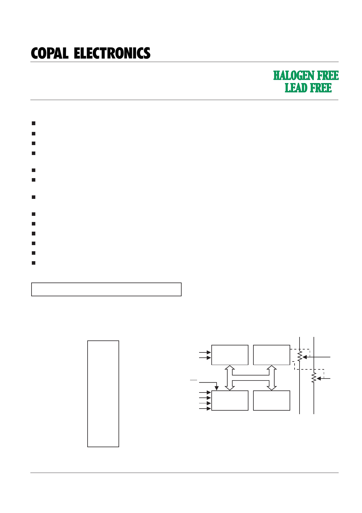
FUNCTIONAL DIAGRAM
SCL
SDA
WP
A0
A1
A2
A3
2-WIRE BUS
INTERFACE
RH0 RH1
WIPER
CONTROL
REGISTERS
RW0
CONTROL
LOGIC
NONVOLATILE
DATA
REGISTERS
RL0 RL1
RW1
© NIDEC COPAL ELECTRONICS CORP.
Characteristics subject to change without notice
1
Doc. No. MD-2123 Rev. D
1 page 
DP7269
POWER UP TIMING (1)(2)
Symbol Parameter
tPUR Power-up to Read Operation
tPUW Power-up to Write Operation
Max
1
1
Units
ms
ms
DP TIMING
Symbol
tWRPO
tWRL
Parameter
Wiper Response Time After Power Supply Stable
Wiper Response Time After Instruction Issued
WRITE CYCLE LIMITS (3)
Symbol Parameter
tWR Write Cycle Time
Max Units
10 µs
10 µs
Max
5
Units
ms
RELIABILITY CHARACTERISTICS
Symbol
NEND(1)
TDR(1)
VZAP(1)
ILTH(1)
Parameter
Endurance
Data Retention
ESD Susceptibility
Latch-Up
Reference Test Method
MIL-STD-883, Test Method 1033
MIL-STD-883, Test Method 1008
MIL-STD-883, Test Method 3015
JEDEC Standard 17
Min
1,000,000
100
2000
100
Max
Units
Cycles/Byte
Years
V
mA
Notes:
(1) This parameter is tested initially and after a design or process change that affects the parameter.
(2) tPUR and tPUW are delays required from the time VCC is stable until the specified operation can be initiated.
(3) The write cycle is the time from a valid stop condition of a write sequence to the end of the internal program/erase cycle. During the write
cycle, the bus interface circuits are disabled, SDA is allowed to remain high, and the device does not respond to its slave address.
Figure 1. Bus Timing
tF tHIGH tR
tLOW
tLOW
SCL
tSU:STA
tHD:DAT
tHD:STA
tSU:DAT
SDA IN
SDA OUT
tAA tDH
tSU:STO
tBUF
© NIDEC COPAL ELECTRONICS CORP.
Characteristics subject to change without notice
5
Doc. No. MD-2123 Rev. D
5 Page 
Figure 10. Increment/Decrement Timing Limits
INC/DEC
Command
Issued
SCL
SDA
RW Voltage Out
tWRL
INSTRUCTION FORMAT
Read Wiper Control Register (WCR)
S DEVICE ADDRESSES A INSTRUCTION A
DATA
AS
T0101 AAAAC1 0 0 1 0 0 PPC7 6 5 4 3 2 1 0 C T
A 3210K
R
10K
KO
P
T
Write Wiper Control Register (WCR)
S DEVICE ADDRESSES A INSTRUCTION A
DATA
AS
T0101 AAAAC1 0 1 0 0 0 PPC7 6 5 4 3 2 1 0 C T
A 3210K
R
10K
KO
P
T
Read Data Register (DR)
S DEVICE ADDRESSES A INSTRUCTION A
DATA
AS
T0101 AAAAC1 0 1 1RRPPC7 6 5 4 3 2 1 0 C T
A 3210K
R
1010K
KO
P
T
Write Data Register (DR)
S DEVICE ADDRESSES A INSTRUCTION A
DATA
AS
T0101 AAAAC1 1 0 0RRPPC7 6 5 4 3 2 1 0 C T
A 3210K
R
1010K
KO
P
T
DP7269
© NIDEC COPAL ELECTRONICS CORP.
Characteristics subject to change without notice
11
Doc. No. MD-2123 Rev. D
11 Page | ||
| Páginas | Total 16 Páginas | |
| PDF Descargar | [ Datasheet DP7269.PDF ] | |
Hoja de datos destacado
| Número de pieza | Descripción | Fabricantes |
| DP7261 | Dual Digital Potentiometers | COPAL ELECTRONICS |
| DP7269 | Dual Digital Potentiometers | COPAL ELECTRONICS |
| Número de pieza | Descripción | Fabricantes |
| SLA6805M | High Voltage 3 phase Motor Driver IC. |
Sanken |
| SDC1742 | 12- and 14-Bit Hybrid Synchro / Resolver-to-Digital Converters. |
Analog Devices |
|
DataSheet.es es una pagina web que funciona como un repositorio de manuales o hoja de datos de muchos de los productos más populares, |
| DataSheet.es | 2020 | Privacy Policy | Contacto | Buscar |