|
|
|
PDF M24C02-R Data sheet ( Hoja de datos )
| Número de pieza | M24C02-R | |
| Descripción | 1-Kbit and 2-Kbit serial I2C bus EEPROMs | |
| Fabricantes | STMicroelectronics | |
| Logotipo | ||
Hay una vista previa y un enlace de descarga de M24C02-R (archivo pdf) en la parte inferior de esta página. Total 30 Páginas | ||
|
No Preview Available !
M24C01/02-W M24C01/02-R
M24C02-F
1-Kbit and 2-Kbit serial I²C bus EEPROMs
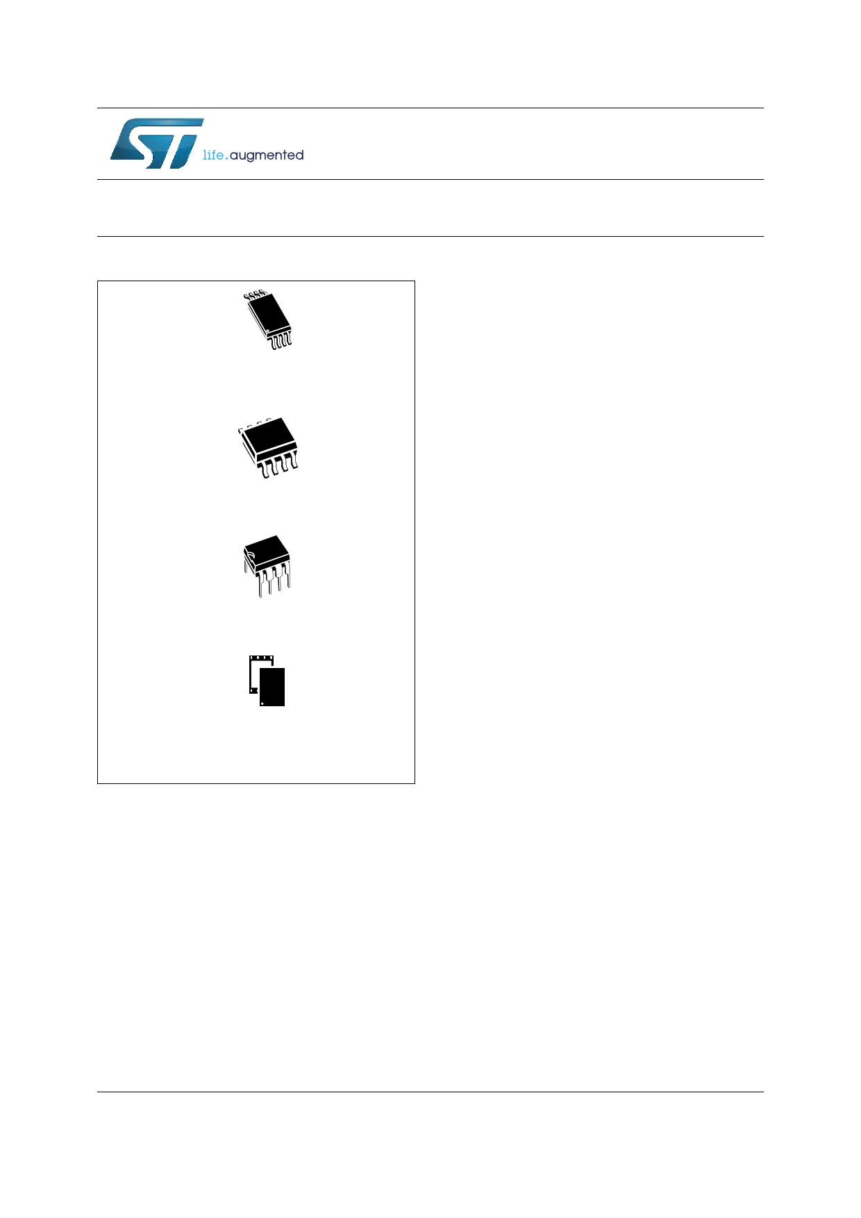
TSSOP8 (DW)
169 mil width
SO8 (MN)
150 mil width
PDIP8 (BN)(1)
UFDFPN8
(MC)
1. Not recommended for new designs
Datasheet - production data
Features
• Compatible with all I2C bus modes:
– 400 kHz
– 100 kHz
• Memory array:
– 1 Kbit (128 bytes) of EEPROM
– 2 Kbit (256 bytes) of EEPROM
– Page size: 16 bytes
• Single supply voltage:
– M24C01/02-W: 2.5 V to 5.5 V
– M24C01/02-R: 1.8 V to 5.5 V
– M24C02-F: 1.7 V to 5.5 V (full temperature
range) and 1.6 V to 1.7 V (limited
temperature range)
• Write:
– Byte Write within 5 ms
– Page Write within 5 ms
• Operating temperature range: from -40 °C up
to +85 °C
• Random and sequential Read modes
• Write protect of the whole memory array
• Enhanced ESD/Latch-Up protection
• More than 4 million Write cycles
• More than 200-year data retention
• Packages:
– RoHS compliant and halogen-free
(ECOPACK®)
September 2013
This is information on a product in full production.
DocID024020 Rev 2
1/34
www.st.com
1 page 
M24C01/02-W M24C01/02-R M24C02-F
List of figures
List of figures
Figure 1.
Figure 2.
Figure 3.
Figure 4.
Figure 5.
Figure 6.
Figure 7.
Figure 8.
Figure 9.
Figure 10.
Figure 11.
Figure 12.
Figure 13.
Figure 14.
Figure 15.
Logic diagram . . . . . . . . . . . . . . . . . . . . . . . . . . . . . . . . . . . . . . . . . . . . . . . . . . . . . . . . . . . . 6
8-pin package connections, top view . . . . . . . . . . . . . . . . . . . . . . . . . . . . . . . . . . . . . . . . . . 6
Block diagram . . . . . . . . . . . . . . . . . . . . . . . . . . . . . . . . . . . . . . . . . . . . . . . . . . . . . . . . . . . . 9
I2C bus protocol . . . . . . . . . . . . . . . . . . . . . . . . . . . . . . . . . . . . . . . . . . . . . . . . . . . . . . . . . 10
Write mode sequences with WC = 0 (data write enabled) . . . . . . . . . . . . . . . . . . . . . . . . . 14
Write mode sequences with WC = 1 (data write inhibited) . . . . . . . . . . . . . . . . . . . . . . . . . 15
Write cycle polling flowchart using ACK . . . . . . . . . . . . . . . . . . . . . . . . . . . . . . . . . . . . . . . 16
Read mode sequences . . . . . . . . . . . . . . . . . . . . . . . . . . . . . . . . . . . . . . . . . . . . . . . . . . . . 17
AC measurement I/O waveform . . . . . . . . . . . . . . . . . . . . . . . . . . . . . . . . . . . . . . . . . . . . . 21
aMnaIx2imC ubmusRabtums vaaxliumeuvmerfsreuqsubeunscypafCra=si4tic00cakpHazci.ta.n.c.e.
(Cbus) for
........
.
.
.
.
.
.
.
.
.
.
.
.
.
.
.
.
.
.
.
27
AC waveforms . . . . . . . . . . . . . . . . . . . . . . . . . . . . . . . . . . . . . . . . . . . . . . . . . . . . . . . . . . 27
TSSOP8 – 8-lead thin shrink small outline, package outline . . . . . . . . . . . . . . . . . . . . . . . 28
SO8N – 8-lead plastic small outline, 150 mils body width, package outline . . . . . . . . . . . . 29
PDIP8 – 8-pin plastic DIP, 0.25 mm lead frame, package outline . . . . . . . . . . . . . . . . . . . 30
UFDFPN8 (MLP8) – package outline (UFDFPN: Ultra thin Fine pitch
Dual Flat Package, No lead) . . . . . . . . . . . . . . . . . . . . . . . . . . . . . . . . . . . . . . . . . . . . . . . . 31
DocID024020 Rev 2
5/34
5
5 Page 
M24C01/02-W M24C01/02-R M24C02-F
Device operation
4.1 Start condition
Start is identified by a falling edge of Serial Data (SDA) while Serial Clock (SCL) is stable in
the high state. A Start condition must precede any data transfer instruction. The device
continuously monitors (except during a Write cycle) Serial Data (SDA) and Serial Clock
(SCL) for a Start condition.
4.2 Stop condition
Stop is identified by a rising edge of Serial Data (SDA) while Serial Clock (SCL) is stable and
driven high. A Stop condition terminates communication between the device and the bus
master. A Read instruction that is followed by NoAck can be followed by a Stop condition to
force the device into the Standby mode.
A Stop condition at the end of a Write instruction triggers the internal Write cycle.
4.3 Data input
During data input, the device samples Serial Data (SDA) on the rising edge of Serial Clock
(SCL). For correct device operation, Serial Data (SDA) must be stable during the rising edge
of Serial Clock (SCL), and the Serial Data (SDA) signal must change only when Serial Clock
(SCL) is driven low.
4.4 Acknowledge bit (ACK)
The acknowledge bit is used to indicate a successful byte transfer. The bus transmitter,
whether it be bus master or slave device, releases Serial Data (SDA) after sending eight bits
of data. During the 9th clock pulse period, the receiver pulls Serial Data (SDA) low to
acknowledge the receipt of the eight data bits.
DocID024020 Rev 2
11/34
33
11 Page | ||
| Páginas | Total 30 Páginas | |
| PDF Descargar | [ Datasheet M24C02-R.PDF ] | |
Hoja de datos destacado
| Número de pieza | Descripción | Fabricantes |
| M24C02-125 | serial I2C bus EEPROM | STMicroelectronics |
| M24C02-A125 | Automotive 2-Kbit serial I2C bus EEPROM | STMicroelectronics |
| M24C02-DRE | 2-Kbit serial I2C bus EEPROM | STMicroelectronics |
| M24C02-F | 1-Kbit and 2-Kbit serial I2C bus EEPROMs | STMicroelectronics |
| Número de pieza | Descripción | Fabricantes |
| SLA6805M | High Voltage 3 phase Motor Driver IC. |
Sanken |
| SDC1742 | 12- and 14-Bit Hybrid Synchro / Resolver-to-Digital Converters. |
Analog Devices |
|
DataSheet.es es una pagina web que funciona como un repositorio de manuales o hoja de datos de muchos de los productos más populares, |
| DataSheet.es | 2020 | Privacy Policy | Contacto | Buscar |