|
|
|
PDF IRFB20N50K Data sheet ( Hoja de datos )
| Número de pieza | IRFB20N50K | |
| Descripción | Power MOSFET ( Transistor ) | |
| Fabricantes | Vishay | |
| Logotipo | ||
Hay una vista previa y un enlace de descarga de IRFB20N50K (archivo pdf) en la parte inferior de esta página. Total 9 Páginas | ||
|
No Preview Available !
IRFB20N50K, SiHFB20N50K
Vishay Siliconix
Power MOSFET
PRODUCT SUMMARY
VDS (V)
RDS(on) (Ω)
Qg (Max.) (nC)
Qgs (nC)
Qgd (nC)
Configuration
500
VGS = 10 V
110
33
54
Single
0.21
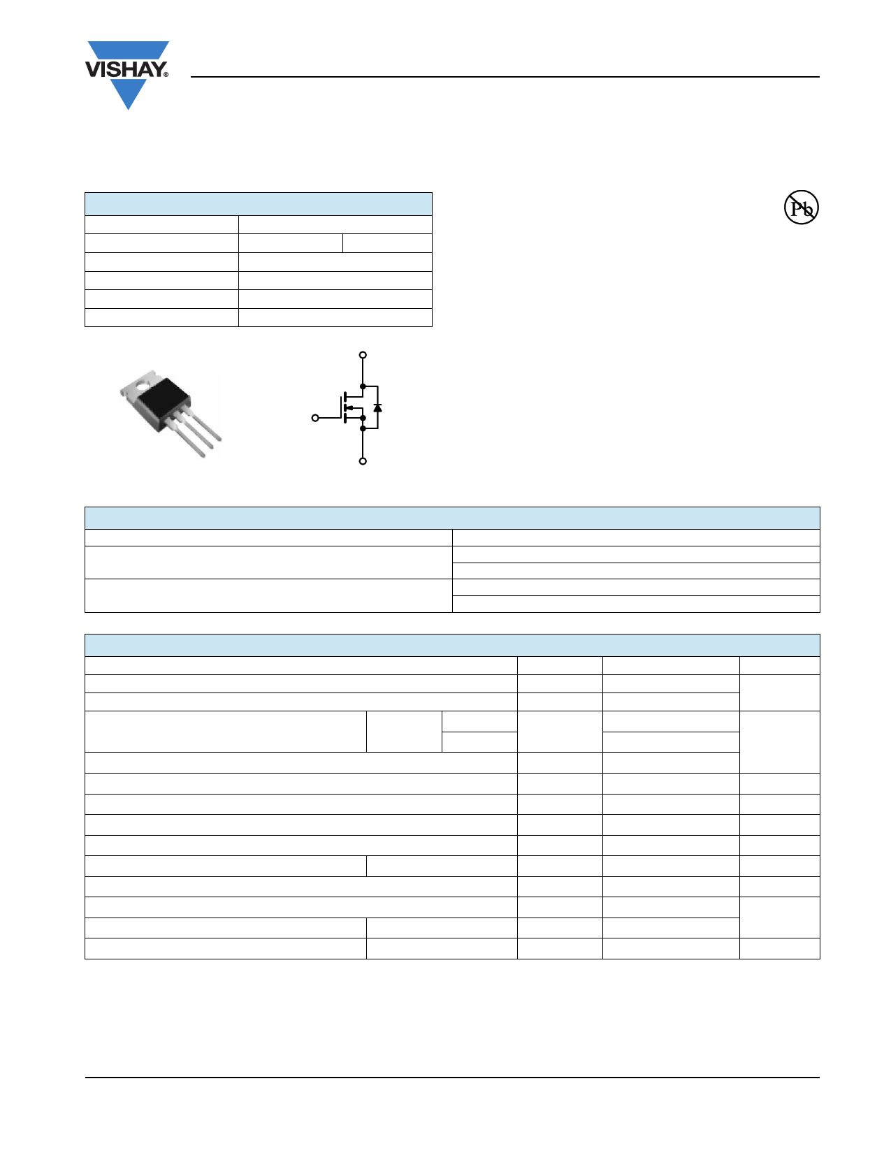
TO-220
D
G
S
D
G
S
N-Channel MOSFET
ORDERING INFORMATION
Package
Lead (Pb)-free
SnPb
FEATURES
• Low Gate Charge Qg Results in Simple Drive
Requirement
• Improved Gate, Avalanche and Dynamic dV/dt
Ruggedness
Available
RoHS*
COMPLIANT
• Fully Characterized Capacitance and Avalanche Voltage
and Current
• Low RDS(on)
• Compliant to RoHS Directive 2002/95/EC
APPLICATIONS
• Switch Mode Power Supply (SMPS)
• Uninterruptible Power Supply
• High Speed Power Switching
• Hard Switched and High Frequency Circuits
TO-220
IRFB20N50KPbF
SiHFB20N50K-E3
IRFB20N50K
SiHFB20N50K
ABSOLUTE MAXIMUM RATINGS TC = 25 °C, unless otherwise noted
PARAMETER
SYMBOL
Drain-Source Voltage
Gate-Source Voltage
Continuous Drain Current
Pulsed Drain Currenta
VGS at 10 V
TC = 25 °C
TC = 100 °C
VDS
VGS
ID
IDM
Linear Derating Factor
Single Pulse Avalanche Energyb
Repetitive Avalanche Currenta
Repetitive Avalanche Energya
EAS
IAR
EAR
Maximum Power Dissipation
Peak Diode Recovery dV/dtc
TC = 25 °C
PD
dV/dt
Operating Junction and Storage Temperature Range
TJ, Tstg
Soldering Recommendations (Peak Temperature)
for 10 s
Mounting Torque
6-32 or M3 screw
Notes
a. Repetitive rating; pulse width limited by maximum junction temperature.
b. Starting TJ = 25 °C, L = 1.6 mH, Rg = 25 Ω, IAS = 20 A.
c. ISD ≤ 20 A, dI/dt ≤ 350 A/µs, VDD ≤ VDS, TJ ≤ 150 °C.
d. 1.6 mm from case.
* Pb containing terminations are not RoHS compliant, exemptions may apply
Document Number: 91101
S09-2236-Rev. D, 05-Apr-10
LIMIT
500
± 30
20
12
80
2.2
330
20
28
280
10
- 55 to + 150
300d
10
UNIT
V
A
W/°C
mJ
A
mJ
W
V/ns
°C
N
www.vishay.com
1
1 page 
IRFB20N50K, SiHFB20N50K
Vishay Siliconix
20
16
12
8
4
0
25 50 75 100 125 150
Fig. 9 - Maximum Drain Current vs. Case Temperature
1
VDS
VGS
Rg
RD
D.U.T.
10 V
Pulse width ≤ 1 µs
Duty factor ≤ 0.1 %
+
- VDD
Fig. 10a - Switching Time Test Circuit
VDS
90 %
10 %
VGS
td(on) tr
td(off) tf
Fig. 10b - Switching Time Waveforms
D = 0.50
0.1 0.20
0.10
0.01
0.01
0.02
0.01
0.001
0.00001
Single Pulse
(Thermal Response)
P DM
Notes:
1. Duty Factor D = t1/t2
2. Peak TJ = PDM x TthJC + TC
t1
t2
0.0001
0.001
0.01
t1, Rectangular Pulse Duration (s)
0.1
Fig. 11 - Maximum Effective Transient Thermal Impedance, Junction-to-Case
1
15 V
VDS
L
Driver
Rg
20 V
tp
D.U.T.
IAS
0.01 Ω
+
- VDAD
A
Fig. 12a - Unclamped Inductive Test Circuit
A
VDS
tp
IAS
Fig. 12b - Unclamped Inductive Waveforms
Document Number: 91101
S09-2236-Rev. D, 05-Apr-10
www.vishay.com
5
5 Page | ||
| Páginas | Total 9 Páginas | |
| PDF Descargar | [ Datasheet IRFB20N50K.PDF ] | |
Hoja de datos destacado
| Número de pieza | Descripción | Fabricantes |
| IRFB20N50K | SMPS MOSFET | International Rectifier |
| IRFB20N50K | Power MOSFET ( Transistor ) | Vishay |
| IRFB20N50KPBF | HEXFET Power MOSFET | International Rectifier |
| Número de pieza | Descripción | Fabricantes |
| SLA6805M | High Voltage 3 phase Motor Driver IC. |
Sanken |
| SDC1742 | 12- and 14-Bit Hybrid Synchro / Resolver-to-Digital Converters. |
Analog Devices |
|
DataSheet.es es una pagina web que funciona como un repositorio de manuales o hoja de datos de muchos de los productos más populares, |
| DataSheet.es | 2020 | Privacy Policy | Contacto | Buscar |