|
|
|
PDF CPC5622 Data sheet ( Hoja de datos )
| Número de pieza | CPC5622 | |
| Descripción | Phone Line Interface IC | |
| Fabricantes | IXYS | |
| Logotipo | ||
Hay una vista previa y un enlace de descarga de CPC5622 (archivo pdf) en la parte inferior de esta página. Total 18 Páginas | ||
|
No Preview Available !
INTEGRATED CIRCUITS DIVISION
CPC5622
LITELINK® III
Phone Line Interface IC (DAA)
Features
• Superior voice solution with low noise and excellent
part-to-part gain accuracy
• 3 kVRMS line isolation
• Simultaneous ringing detection and CID monitoring
for worldwide applications
• Provides both full-wave ringing detect and half-wave
ringing detect for maximum versatility
• Transmit power of up to +10 dBm into 600
• Data access arrangement (DAA) solution for modem
speeds up to V.92
• 3.3V or 5 V power supply operation
• Easy interface with modem ICs and voice CODECs
• Worldwide dial-up telephone network compatibility
• CPC5622 can be used in circuits that comply with
the requirements of TIA/EIA/IS-968 (FCC part 68),
UL60950 (UL1950), EN/IEC 60950-1
Supplementary Isolation Compliant, IEC60950,
EN55022B, CISPR22B, EN55024, and TBR-21
• Line-side circuit powered from telephone line
• Compared to other silicon DAA solutions, LITELINK:
- Uses fewer passive components
- Takes up less printed-circuit board space
- Uses less telephone line power
- Is a single-IC solution
Applications
• Computer telephony and gateways, such as VoIP
• PBXs
• Satellite and cable set-top boxes
• V.92 (and other standard) modems
• Fax machines
• Voicemail systems
• Embedded modems for POS terminals, automated
banking, remote metering, vending machines,
security, and surveillance
Description
LITELINK III is a single-package silicon phone line
interface (PLI) DAA used in voice and data
communication applications to make connections
between low-voltage equipment and high-voltage
telephone networks.
LITELINK uses on-chip optical components and a few
inexpensive external components to form the required
high voltage isolation barrier. LITELINK eliminates the
need for large isolation transformers or capacitors
used in other phone line interface configurations.
LITELINK also provides AC and DC phone line
terminations, switchhook, 2-wire to 4-wire hybrid,
ringing detection, and full time receive on-hook
transmission capability.
The CPC5622 is a member of, and builds upon, IXYS
Integrated Circuits Division’s third generation of
LITELINK products with improved insertion loss
performance and lower minimum current draw from
the phone line. The CPC5622 version of LITELINK III
provides concurrent ringing detection and CID
monitoring for world wide applications. Both half-wave
and full-wave ringing detection are provided for
maximum versatility.
Ordering Information
Part Number
CPC5622A
CPC5622ATR
Description
32-Pin SOIC Phone Line Interface, 50/tube
32-Pin SOIC Phone Line Interface,
tape and reel, 1000/reel
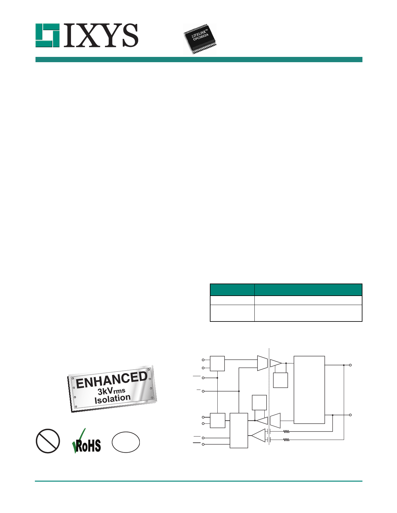
CPC5622 Block Diagram
Isolation Barrier
Is3oklVartmiosn
Pb e3
Tx+
Tx-
MODE
Transmit
Diff.
Amplifier
OH
Transmit
Isolation
Amplifier
Tx.
Gain
Trim
Rx.
Gain
Trim
Rx+ Receive
Diff.
Rx- Amplifier
Ringing Detect Outputs
RING
Half Wave
Rx Amp
&
Ringing Det.
RING2
Full Wave
Snoop
Amplifier
Receive
Isolation
Amplifier
CSNOOP
RSNOOP
CSNOOP
RSNOOP
Transconductance
Stage
2-4 Wire Hybrid
AC/DC Termination
Hook Switch
TIP
RING
DS-CPC5622-R03
www.ixysic.com
1
1 page 
INTEGRATED CIRCUITS DIVISION
1.3 Pin Description
Pin Name
1 VDD
2 TXSM
3 TX-
4 TX+
5 TX
6 MODE
7 GND
8 OH
9 RING
10 RING2
11 RX-
12 RX+
13 SNP+
14 SNP-
15 RXF
16 RX
17 VDDL
18 RXS
19 RPB
20 BR-
21 ZDC
22 DCS2
23 DCS1
24 NTF
25 GAT
26 NTS
27 BR-
28 TXSL
29 ZNT
30 ZTX
31 TXF
32 REFL
Function
Low-voltage (CPE) side power supply
Transmit summing junction
Negative differential transmit signal to DAA
from low-voltage side
Positive differential transmit signal to DAA from
low-voltage side
Transmit differential amplifier output
When asserted low, changes gain of TX path
(-7 dB) and RX path (+7 dB) to accommodate
reactive termination networks
Low-voltage (CPE) side analog ground
Assert logic low for off-hook operation
Half wave ringing detect output signal
Full wave ringing detect output signal
Negative differential analog signal received
from the telephone line. Must be AC coupled
with 0.1 F.
Positive differential analog signal received from
the telephone line. Must be AC coupled with
0.1 F.
Positive differential snoop input
Negative differential snoop input
Receive photodiode amplifier output
Receive photodiode summing junction
Power supply for line side, regulated from tip
and ring.
Receive isolation amp summing junction
Receive LED pre-bias current set
Bridge rectifier return
Electronic inductor DCR/current limit
DC feedback output
V to I slope control
Network amplifier feedback
External MOSFET gate control
Receive signal input
Bridge rectifier return
Transmit photodiode summing junction
Receiver impedance set
Transmit transconductance gain set
Transmit photodiode amplifier output
1.25 VDC reference
Figure 1. Pinout
1 VDD
2 TXSM
3 TX-
4 TX+
5 TX
6 MODE
7 GND
8 OH
9 RING
10 RING2
11 RX-
12 RX+
13 SNP+
14 SNP-
15 RXF
16 RX
R03 www.ixysic.com
CPC5622
REFL
TXF
ZTX
ZNT
TXSL
BR-
NTS
GAT
NTF
DCS1
DCS2
ZDC
BR-
RPB
RXS
VDDL
32
31
30
29
28
27
26
25
24
23
22
21
20
19
18
17
5
5 Page 
INTEGRATED CIRCUITS DIVISION
will output one logic low pulse per cycle of the ringing
frequency. Also, because the RING2 is the output of a
full-wave detector it will output two logic low pulses
per cycle of the ringing frequency. Hence, the
nomenclature RING2 for twice the output pulses.
The set-up of the ringing detector comparator causes
the RING output pulses to remain low for most of one
half-cycle of the ringing signal and remains high for the
entire second half-cycle of the ringing signal. For the
RING2 output, the pulses remain low during most of
both halves of the ringing cycle and returns high for
only a short period near the zero-crossing of the
ringing signal. Both of the ringing outputs remain high
during the silent interval between ringing bursts.
Hysteresis is employed in the LITELINK ringing
detector circuit to improve noise immunity.
The ringing detection threshold depends on the values
of R3 (RSNPD), R6 & R44 (RSNP-), R7 & R45 (RSNP+),
C7 (CSNP-), and C8 (CSNP+). The value of these
components shown in the application circuits are
recommended for typical operation. The ringing
detection threshold can be changed according to the
following formula:
VRINGPK
=
7-R---5-S--0-N--m-P---D-V--
RSNPTOTAL + RSNPD2 + -------f--R---I--N---G-1---C----S---N---P------2
Where:
• RSNPD = R3 in the application circuits shown in this
data sheet.
• RSNPTOTAL = the total of R6, R7, R44, and R45 in
the application circuits shown in this data sheet.
• CSNP = C7 = C8 in the application circuits shown in
this data sheet.
• And ƒRING is the frequency of the ringing signal.
IXYS Integrated Circuits Division Application Note
AN-117 Customize Caller ID Gain and Ring Detect Voltage
Threshold is a spreadsheet for trying different
component values in this circuit. Changing the ringing
detection threshold will also change the caller ID gain
and the timing of the polarity reversal detection pulse,
if used.
CPC5622
3.2.2 Polarity Reversal Detection in On-hook
State
The full-wave ringing detector in the CPC5622 makes
it possible to detect an on-hook tip and ring battery
polarity reversal using the RING2 output. When the
polarity of the battery voltage applied to tip and ring
reverses, a pulse on RING2 indicates the event. The
system logic must be able to discriminate a single
pulse of approximately 1 msec when using the
recommended external snoop circuit components
from a valid ringing signal.
3.2.3 On-hook Caller ID Signal Reception
On-hook Caller IDentity (CID) data burst signals are
coupled through the snoop components, buffered
through LITELINK and output at the RX+ and RX-
pins.
In North America, CID data signals are typically sent
between the first and second ringing signal while in
other countries the CID information may arrive prior to
any other signalling state.
In applications that transmit CID after the first ringing
burst such as in North American, follow these steps to
receive on-hook caller ID data via the LITELINK RX
outputs:
1. Detect the first full ringing signal burst on RING
or RING2.
2. Monitor and process the CID data from the RX
outputs.
For applications as in China and Brazil where CID may
arrive prior to ringing, follow these steps to receive
on-hook caller ID data via the LITELINK RX outputs:
1. Simultaneously monitor for CID data from the RX
outputs and for ringing on RING or RING2.
2. Process the appropriate signalling data.
Note: Taking LITELINK off-hook (via the OH pin)
disconnects the snoop path from the receive outputs
and disables the ringing detector outputs RING and
RING2.
CID gain from tip and ring to RX+ and RX- is
determined by:
R03 www.ixysic.com
11
11 Page | ||
| Páginas | Total 18 Páginas | |
| PDF Descargar | [ Datasheet CPC5622.PDF ] | |
Hoja de datos destacado
| Número de pieza | Descripción | Fabricantes |
| CPC5620 | Phone Line Interface IC | IXYS |
| CPC5620 | (CPC5620 / CPC5621) Phone Line Interface IC | Clare |
| CPC5621 | Phone Line Interface IC | IXYS |
| CPC5621 | (CPC5620 / CPC5621) Phone Line Interface IC | Clare |
| Número de pieza | Descripción | Fabricantes |
| SLA6805M | High Voltage 3 phase Motor Driver IC. |
Sanken |
| SDC1742 | 12- and 14-Bit Hybrid Synchro / Resolver-to-Digital Converters. |
Analog Devices |
|
DataSheet.es es una pagina web que funciona como un repositorio de manuales o hoja de datos de muchos de los productos más populares, |
| DataSheet.es | 2020 | Privacy Policy | Contacto | Buscar |