|
|
PDF IS43DR16640C Data sheet ( Hoja de datos )
| Número de pieza | IS43DR16640C | |
| Descripción | DDR2 DRAM | |
| Fabricantes | ISSI | |
| Logotipo |  |
|
Hay una vista previa y un enlace de descarga de IS43DR16640C (archivo pdf) en la parte inferior de esta página. Total 30 Páginas | ||
|
No Preview Available !
IS43/46DR81280C
IS43/46DR16640C
128Mx8, 64Mx16 DDR2 DRAM
FEATURES
• Vdd = 1.8V ±0.1V, Vddq = 1.8V ±0.1V
• JEDEC standard 1.8V I/O (SSTL_18-compatible)
• Double data rate interface: two data transfers
per clock cycle
• Differential data strobe (DQS, DQS)
• 4-bit prefetch architecture
• On chip DLL to align DQ and DQS transitions
with CK
• 8 internal banks for concurrent operation
• Programmable CAS latency (CL) 3, 4, 5, 6 and 7
supported
• Posted CAS and programmable additive latency
(AL) 0, 1, 2, 3, 4, 5 and 6 supported
• WRITE latency = READ latency - 1 tCK
• Programmable burst lengths: 4 or 8
• Adjustable data-output drive strength, full and
reduced strength options
• On-die termination (ODT)
ADVANCED INFORMATION
DESCRIPTION
MAY 2013
ISSI's 1Gb DDR2 SDRAM uses a double-data-rate
architecture to achieve high-speed operation. The
double-data rate architecture is essentially a 4n-prefetch
architecture, with an interface designed to transfer two
data words per clock cycle at the I/O balls.
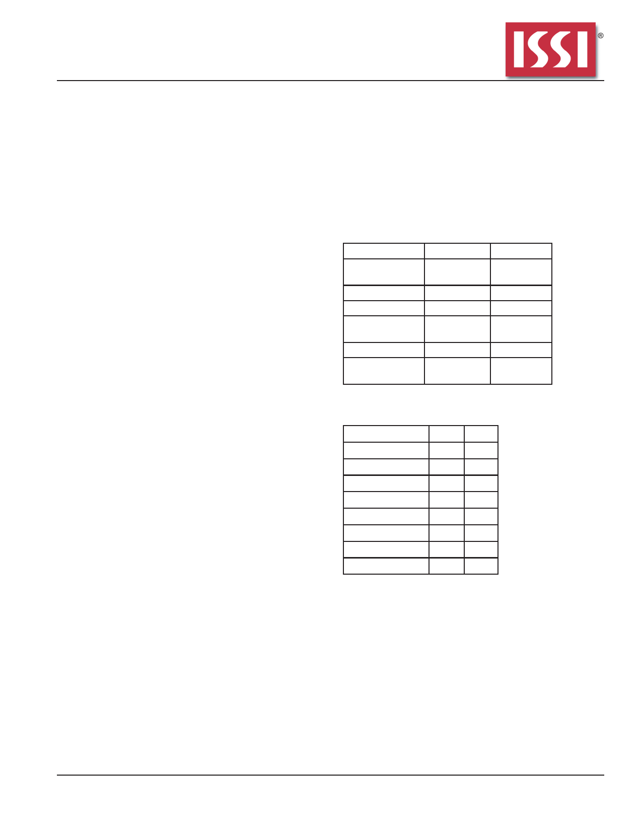
ADDRESS TABLE
Parameter
Configuration
Refresh Count
128M x 8
16M x 8 x 8
banks
8K/64ms
64M x 16
8M x 16 x 8
banks
8K/64ms
Row Addressing 16K (A0-A13) 8K (A0-A12)
Column
Addressing
1K (A0-A9)
Bank Addressing BA0 - BA2
1K (A0-A9)
BA0 - BA2
Precharge
Addressing
A10
A10
OPTIONS
• Configuration(s):
128Mx8 (16Mx8x8 banks): IS43/46DR81280C
64Mx16 (8Mx16x8 banks): IS43/46DR16640C
• Package:
x8: 60-ball BGA (8mm x 10.5mm)
x16: 84-ball WBGA (8mm x 12.5mm)
• Timing – Cycle time
2.5ns @CL=5 DDR2-800D
2.5ns @CL=6 DDR2-800E
3.0ns @CL=5 DDR2-667D
3.75ns @CL=4 DDR2-533C
5ns @CL=3 DDR2-400B
• Temperature Range:
Commercial (0°C ≤ Tc ≤ 85°C)
Industrial (-40°C ≤ Tc ≤ 95°C; -40°C ≤ Ta ≤ 85°C)
Automotive, A1 (-40°C ≤ Tc ≤ 95°C; -40°C ≤ Ta ≤ 85°C)
Automotive, A2 (-40°C ≤ Tc; Ta ≤ 105°C)
Tc = Case Temp, Ta = Ambient Temp
KEY TIMING PARAMETERS
Speed Grade -25D -3D
tRCD
12.5 15
tRP 12.5 15
tRC 55 55
tRAS
40 40
tCK @CL=3
55
tCK @CL=4
3.75 3.75
tCK @CL=5
2.5 3
tCK @CL=6
2.5 —
Copyright © 2013 Integrated Silicon Solution, Inc. All rights reserved. ISSI reserves the right to make changes to this specification and its products at any time without
notice. ISSI assumes no liability arising out of the application or use of any information, products or services described herein. Customers are advised to obtain the latest
version of this device specification before relying on any published information and before placing orders for products.
Integrated Silicon Solution, Inc. does not recommend the use of any of its products in life support applications where the failure or malfunction of the product can reason-
ably be expected to cause failure of the life support system or to significantly affect its safety or effectiveness. Products are not authorized for use in such applications
unless Integrated Silicon Solution, Inc. receives written assurance to its satisfaction, that:
a.) the risk of injury or damage has been minimized;
b.) the user assume all such risks; and
c.) potential liability of Integrated Silicon Solution, Inc is adequately protected under the circumstances
Integrated Silicon Solution, Inc. — www.issi.com 1
Rev. 00A
6/4/2013
1 page 
IS43/46DR81280C, IS43/46DR16640C
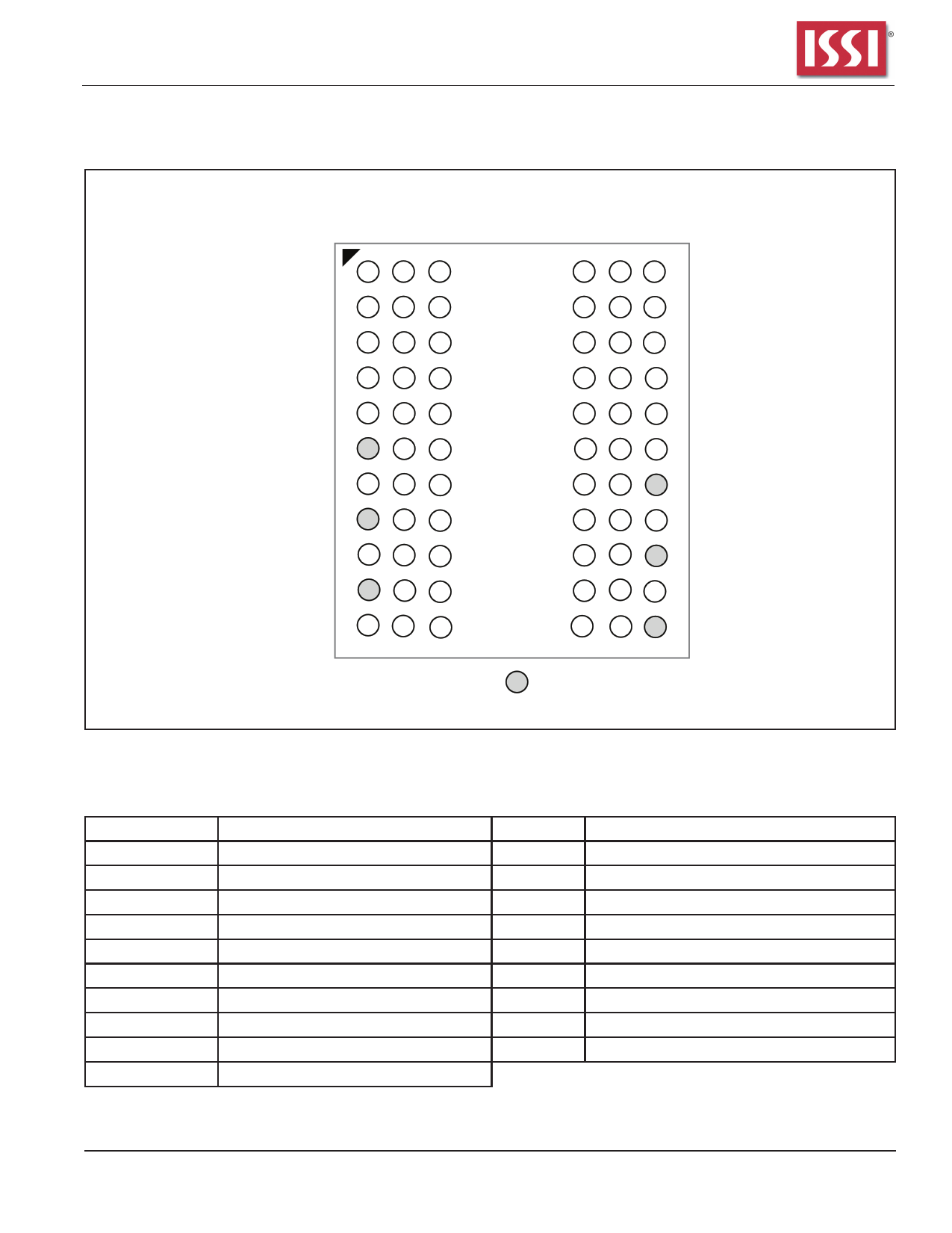
PIN CONFIGURATION
PACKAGE CODE: B 60 BALL FBGA (Top View) (8.00 mm x 10.5 mm Body, 0.8 mm Ball Pitch)
123456789
A
B VDD RDQS VSS
C DQ6 VSSQ DM/RDQS
D VDDQ DQ1 VDDQ
E DQ4 VSSQ DQ3
F VDDL VREF VSS
G CKE WE
H BA2 BA0 BA1
J A10 A1
K VSS A3 A5
L A7 A9
VDD A12 NC
VSSQ DQS VDDQ
DQS VSSQ DQ7
VDDQ DQ0 VDDQ
DQ2 VSSQ DQ5
VSSDL CK VDD
RAS CK ODT
CAS CS
A2 A0 VDD
A6 A4
A11 A8 VSS
NC A13
Not populated
Pin name
A0 to A13
BA0 to BA2
DQ0 to DQ7
DQS, /DQS
/CS
/RAS, /CAS, /WE
CKE
CK, /CK
DM
RDQS, /RDQS
Function
Address inputs
Bank select
Data input/output
Differential data strobe
Chip select
Command input
Clock enable
Differential clock input
Write data mask
Differential Redundant Data Strobe
Pin name
ODT
VDD
VSS
VDDQ
VSSQ
VREF
VDDL
VSSDL
NC
Function
ODT control
Supply voltage for internal circuit
Ground for internal circuit
Supply voltage for DQ circuit
Ground for DQ circuit
Input reference voltage
Supply voltage for DLL circuit
Ground for DLL circuit
No connection
Integrated Silicon Solution, Inc. — www.issi.com 5
Rev. 00A
6/4/2013
5 Page 
IS43/46DR81280C, IS43/46DR16640C
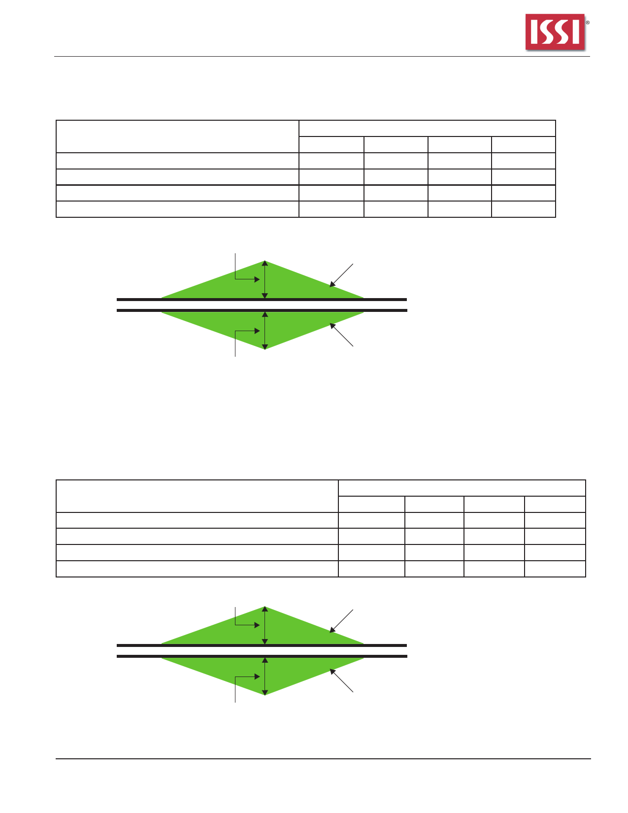
OVERSHOOT/UNDERSHOOT SPECIFICATION
AC overshoot/undershoot specification for Address and Control pins
Parameter
Maximum peak amplitude allowed for overshoot area
Maximum peak amplitude allowed for undershoot area
Maximum overshoot area above VDD (see figure below)
Maximum undershoot area below VSS (see figure below)
DDR2-400
0.5V
0.5V
1.33 V-ns
1.33 V-ns
Specification
DDR2-533 DDR2-667
0.5V 0.5V
0.5V 0.5V
1.0 V-ns
0.8 V-ns
1.0 V-ns
0.8 V-ns
DDR2-800
0.5V
0.5V
0.66 V-ns
0.66 V-ns
Maximum Amplitude
Overshoot Area
Volts
(V)
VDD
VSS
Maximum Amplitude
Time (ns)
AC overshoot and undershoot definition for address and control pins
Undershoot Area
AC overshoot/undershoot specification for Clock, Data, Strobe, and Mask pins:
DQ, (U/L/R) DQS, (U/L/R) DQS, DM, CK, CK
Parameter
Maximum peak amplitude allowed for overshoot area
Maximum peak amplitude allowed for undershoot area
Maximum overshoot area above VDDQ (See Figure below)
Maximum undershoot area below VSSQ (See Figure below)
DDR2-400
0.5V
0.5V
0.38 V-ns
0.38 V-ns
Specification
DDR2-533 DDR2-667
0.5V
0.5V
0.5V
0.5V
0.28 V-ns 0.23 V-ns
0.28 V-ns 0.23 V-ns
DDR2-800
0.5V
0.5V
0.23 V-ns
0.23 V-ns
Maximum Amplitude
Overshoot Area
Volts
(V)
VDDQ
VSSQ
Maximum Amplitude
Time (ns)
Undershoot Area
AC overshoot and undershoot definition for clock, data, strobe, and mask pins
Integrated Silicon Solution, Inc. — www.issi.com 11
Rev. 00A
6/4/2013
11 Page | ||
| Páginas | Total 30 Páginas | |
| PDF Descargar | [ Datasheet IS43DR16640C.PDF ] | |
Hoja de datos destacado
| Número de pieza | Descripción | Fabricantes |
| IS43DR16640C | DDR2 DRAM | ISSI |
| Número de pieza | Descripción | Fabricantes |
| SLA6805M | High Voltage 3 phase Motor Driver IC. |
Sanken |
| SDC1742 | 12- and 14-Bit Hybrid Synchro / Resolver-to-Digital Converters. |
Analog Devices |
|
DataSheet.es es una pagina web que funciona como un repositorio de manuales o hoja de datos de muchos de los productos más populares, |
| DataSheet.es | 2020 | Privacy Policy | Contacto | Buscar |
