|
|
PDF IS43R16160 Data sheet ( Hoja de datos )
| Número de pieza | IS43R16160 | |
| Descripción | 256Mb Synchronous DRAM | |
| Fabricantes | Integrated Silicon Solution | |
| Logotipo | ||
Hay una vista previa y un enlace de descarga de IS43R16160 (archivo pdf) en la parte inferior de esta página. Total 30 Páginas | ||
|
No Preview Available !
IS43R16160
32Mx8, 16Mx16
256Mb Synchronous DRAM
FEATURES:
• Vdd =Vddq = 2.5V+0.2V (-5, -6, -75)
• Double data rate architecture ; two data transfers
per clock cycle.
• Bidirectional , data strobe (DQS) is transmitted/
received with data
• Differential clock input (CLK and /CLK)
• DLL aligns DQ and DQS transitions with CLK
transitions edges of DQS
• Commands entered on each positive CLK edge;
• Data and data mask referenced to both edges of
DQS
• 4 bank operation controlled by BA0 , BA1
(Bank Address)
• /CAS latency -2.0 / 2.5 / 3.0 (programmable) ;
Burst length -2 / 4 / 8 (programmable)
Burst type -Sequential / Interleave (program-
mable)
• Auto precharge/ All bank precharge controlled
by A10
• 8192 refresh cycles / 64ms (4 banks concurrent
refresh)
• Auto refresh and Self refresh
• Row address A0-12 / Column address A0-8(x16)
• SSTL_2 Interface
• Package 400-mil, 66-pin Thin Small Outline
Package (TSOP II) with 0.65mm lead pitch
• Temperature Range:
Commercial (0oC to +70oC)
PRELIMINARY INFORMATION
OCTOBER 2008
DESCRIPTION:
IS43R16160 is a 4-bank x 4,194,304-word x 16bit
double data rate synchronous DRAM , with SSTL_2
interface. All control and address signals are referenced
to the rising edge of CLK. Input data is registered on
both edges of data strobe, and output data and data
strobe are referenced on both edges of CLK. The device
achieves very high speed clock rate up to 200 MHz.
KEY TIMING PARAMETERS
Parameter
-5 -6 -75 Unit
Clk Cycle Time
CAS Latency = 3 5 6 7.5 ns
CAS Latency = 2.5 5
6 7.5 ns
CAS Latency = 2 7.5 7.5 7.5 ns
Clk Frequency
CAS Latency = 3 200 167 143 MHz
CAS Latency = 2.5 200 167 143 MHz
CAS Latency = 2 143 143 143 MHz
Access Time from Clock
CAS Latency = 3 +0.70 +0.70 +0.75 ns
CAS Latency = 2.5 +0.70 +0.70 +0.75 ns
CAS Latency = 2 +0.75 +0.75 +0.75 ns
ADDRESS TABLE
Parameter
16M x 16
Configuration
4M x 16 x 4 banks
Bank Address Pins BA0, BA1
Autoprecharge Pins A10/AP
Row Addresses
A0 – A12
Column Addresses A0 – A8
Refresh Count
8192 / 64ms
Copyright © 2006 Integrated Silicon Solution, Inc. All rights reserved. ISSI reserves the right to make changes to this specification and its products at any time without
notice. ISSI assumes no liability arising out of the application or use of any information, products or services described herein. Customers are advised to obtain the
latest version of this device specification before relying on any published information and before placing orders for products.
Integrated Silicon Solution, Inc.
Rev. 00A
09/10/08
1
1 page 
IS43R16160
Preliminary
Zentel Electronics Corporation
A3S56D30/40ETP
256M Double Data Rate Synchronous DRAM
BASIC FUNCTIONS
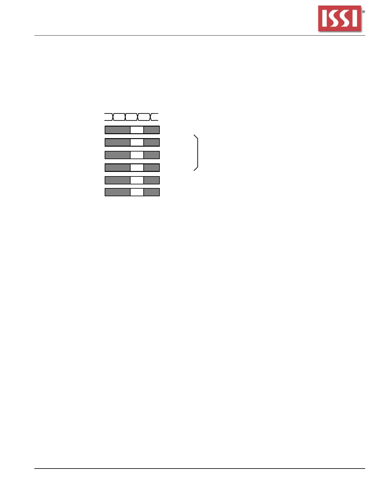
ISSI's 256-Mbit DDR SDRAM provides basic functions, bank (row) activate, burst read / write, bank
(row) precharge, and auto / self refresh. Each command is defined by control signals of /RAS,
/CAS and /WE at CLK rising edge. In addition to 3 signals, /CS , CKE and A10 are used as chip
select, refresh option, and precharge option, respectively. To know the detailed definition of
commands, please see the command truth table.
/CLK
CLK
/CS
Chip Select : L=select, H=deselect
/RAS
Command
/CAS
Command
define basic commands
/WE Command
CKE
Refresh Option @refresh command
A10 Precharge Option @precharge or read/write command
Activate (ACT) [/RAS =L, /CAS =/WE =H]
ACT command activates a row in an idle bank indicated by BA.
Read (READ) [/RAS =H, /CAS =L, /WE =H]
READ command starts burst read from the active bank indicated by BA. First output data appears after
/CAS latency. When A10 =H at this command, the bank is deactivated after the burst read (auto-
precharge, READA)
Write (WRITE) [/RAS =H, /CAS =/WE =L]
WRITE command starts burst write to the active bank indicated by BA. Total data length to be written
is set by burst length. When A10 =H at this command, the bank is deactivated after the burst write
(auto-precharge, WRITEA)
Precharge (PRE) [/RAS =L, /CAS =H, /WE =L]
PRE command deactivates the active bank indicated by BA. This command also terminates burst read
/write operation. When A10 =H at this command, all banks are deactivated (precharge all, PREA ).
Auto-Refresh (REFA) [/RAS =/CAS =L, /WE =CKE =H]
REFA command starts auto-refresh cycle. Refresh address including bank address are generated
internally. After this command, the banks are precharged automatically.
IDntDegRraSteDdRSAiliMco(nRSeovlu.1ti.o1n), Inc.
Rev. 00A
09/10/08
5
5 Page 
IS43R16160
Preliminary
Zentel Electronics Corporation
A3S56D30/40ETP
256M Double Data Rate Synchronous DRAM
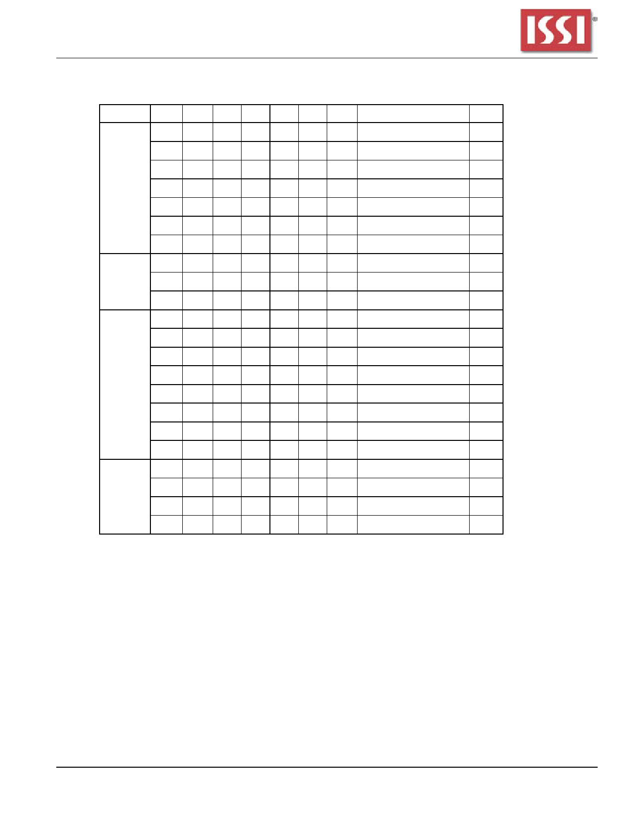
FUNCTION TRUTH TABLE for CKE
Current State CKE n-1 CKE n /CS
SELF-
REFRESHING
H
L
XX
HH
L HL
L HL
L HL
L HL
L LX
POWER H X X
DOWN
L HX
L LX
ALL BANKS
IDLE
H
H
HX
LL
H LH
H LL
H LL
H LL
H LL
L XX
ANY STATE
other than listed
above
H
H
L
HX
LX
HX
L LX
/RAS
X
X
H
H
H
L
X
X
X
X
X
L
X
H
H
H
L
X
X
X
X
X
/CAS
X
X
H
H
L
X
X
X
X
X
X
L
X
H
H
L
X
X
X
X
X
X
/WE Address
Action
X X INVALID
X X Exit Self-Refresh (Idle after tRC)
H X Exit Self-Refresh (Idle after tRC)
L X ILLEGAL
X X ILLEGAL
X X ILLEGAL
X X NOP (Maintain Self-Refresh)
X X INVALID
X X Exit Power Down to Idle
X X NOP (Maintain Self-Refresh)
X X Refer to Function Truth Table
H X Enter Self-Refresh
X X Enter Power Down
H X Enter Power Down
L X ILLEGAL
X X ILLEGAL
X X ILLEGAL
X X Refer to Current State =Power Down
X X Refer to Function Truth Table
X X Begin CLK Suspend at Next Cycle
X X Exit CLK Suspend at Next Cycle
X X Maintain CLK Suspend
Notes
1
1
1
1
1
1
1
2
2
2
2
2
2
2
2
3
3
ABBREVIATIONS:
H=High Level, L=Low Level, X=Don't Care
NOTES:
1. CKE Low to High transition will re-enable CLK and other inputs asynchronously.
A minimum setup time must be satisfied before any command other than EXIT.
2. Power-Down and Self-Refresh can be entered only from the All Banks Idle State.
3. Must be legal command.
DInDteRgrSatDedRSAiMlico(Rn eSvo.lu1t.i1o)n, Inc.
Rev. 00A
09/10/08
11
11 Page | ||
| Páginas | Total 30 Páginas | |
| PDF Descargar | [ Datasheet IS43R16160.PDF ] | |
Hoja de datos destacado
| Número de pieza | Descripción | Fabricantes |
| IS43R16160 | 256Mb Synchronous DRAM | Integrated Silicon Solution |
| IS43R16160A | 16Meg x 16 256-MBIT DDR SDRAM | Integrated Silicon Solution |
| IS43R16160D | DDR SDRAM | ISSI |
| IS43R16160F | 256Mb DDR SDRAM | Integrated Silicon Solution |
| Número de pieza | Descripción | Fabricantes |
| SLA6805M | High Voltage 3 phase Motor Driver IC. |
Sanken |
| SDC1742 | 12- and 14-Bit Hybrid Synchro / Resolver-to-Digital Converters. |
Analog Devices |
|
DataSheet.es es una pagina web que funciona como un repositorio de manuales o hoja de datos de muchos de los productos más populares, |
| DataSheet.es | 2020 | Privacy Policy | Contacto | Buscar |
