|
|
PDF IS43R32400D Data sheet ( Hoja de datos )
| Número de pieza | IS43R32400D | |
| Descripción | 128Mb DDR SDRAM | |
| Fabricantes | Integrated Silicon Solution | |
| Logotipo | ||
Hay una vista previa y un enlace de descarga de IS43R32400D (archivo pdf) en la parte inferior de esta página. Total 30 Páginas | ||
|
No Preview Available !
IS43R32400D
4Mx32
128Mb DDR SDRAM
SEPTEMBER 2011
FEATURES
• Double-data rate architecture; two data transfers
per clock cycle
• Bidirectional, data strobe (DQS) is transmitted/
received with data, to be used in capturing data
at the receiver
• DQS is edge-aligned with data for READs and
centre-aligned with data for WRITEs
• Differential clock inputs (CK and CK)
• DLL aligns DQ and DQS transitions with CK
transitions
• Commands entered on each positive CK edge;
data and data mask referenced to both edges of
DQS
• Four internal banks for concurrent operation
• Data Mask for write data. DM masks write data
at both rising and falling edges of data strobe
• Burst Length: 2, 4 and 8
• Burst Type: Sequential and Interleave mode
• Programmable CAS latency: 2, 2.5, 3 and 4
• Auto Refresh and Self Refresh Modes
• Auto Precharge
• VDD and VDDQ: 2.5V ± 0.2V (-5, -6)
• VDD and VDDQ: 2.5V ± 0.125V (-4)
• SSTL_2 compatible I/O
OPTIONS
• Configuration(s): 4M x32
• Package(s):
144 Ball BGA (x32)
• Lead-free package available
• Temperature Range:
Commercial (0°C to +70°C)
Industrial (-40°C to +85°C)
DEVICE OVERVIEW
ISSI’s 128-Mbit DDR SDRAM achieves high speed data
transfer using pipeline architecture and two data word
accesses per clock cycle. The 134,217,728-bit memory
array is internally organized as four banks of 32Mb to
allow concurrent operations. The pipeline allows Read
and Write burst accesses to be virtually continuous, with
the option to concatenate or truncate the bursts. The
programmable features of burst length, burst sequence
and CAS latency enable further advantages. The
device is available in 32-bit data word size Input data is
registered on the I/O pins on both edges of Data Strobe
signal(s), while output data is referenced to both edges
of Data Strobe and both edges of CLK. Commands are
registered on the positive edges of CLK.
An Auto Refresh mode is provided, along with a Self
Refresh mode. All I/Os are SSTL_2 compatible.
ADDRESS TABLE
Parameter
4M x 32
Configuration
1M x 32 x 4 banks
Bank Address
Pins
BA0, BA1
Autoprecharge
Pins
A8/AP
Row Addresses 4K(A0 – A11)
Column Address 256(A0 – A7)
Refresh Count
4K / 32ms
KEY TIMING PARAMETERS
Speed Grade
-4 -5 -6 Units
Fck Max CL = 4
250 200 166 MHz
Fck Max CL = 3
200 200 166 MHz
Fck Max CL = 2.5
– 166 166 MHz
Fck Max CL = 2
– 133 133 MHz
Copyright © 2011 Integrated Silicon Solution, Inc. All rights reserved. ISSI reserves the right to make changes to this specification and its products at any time without
notice. ISSI assumes no liability arising out of the application or use of any information, products or services described herein. Customers are advised to obtain the lat-
est version of this device specification before relying on any published information and before placing orders for products.
Integrated Silicon Solution, Inc. does not recommend the use of any of its products in life support applications where the failure or malfunction of the product can reason-
ably be expected to cause failure of the life support system or to significantly affect its safety or effectiveness. Products are not authorized for use in such applications
unless Integrated Silicon Solution, Inc. receives written assurance to its satisfaction, that:
a.) the risk of injury or damage has been minimized;
b.) the user assume all such risks; and
c.) potential liability of Integrated Silicon Solution, Inc is adequately protected under the circumstances
Integrated Silicon Solution, Inc.
Rev. A
09/07/2011
1
1 page 
IS43R32400D
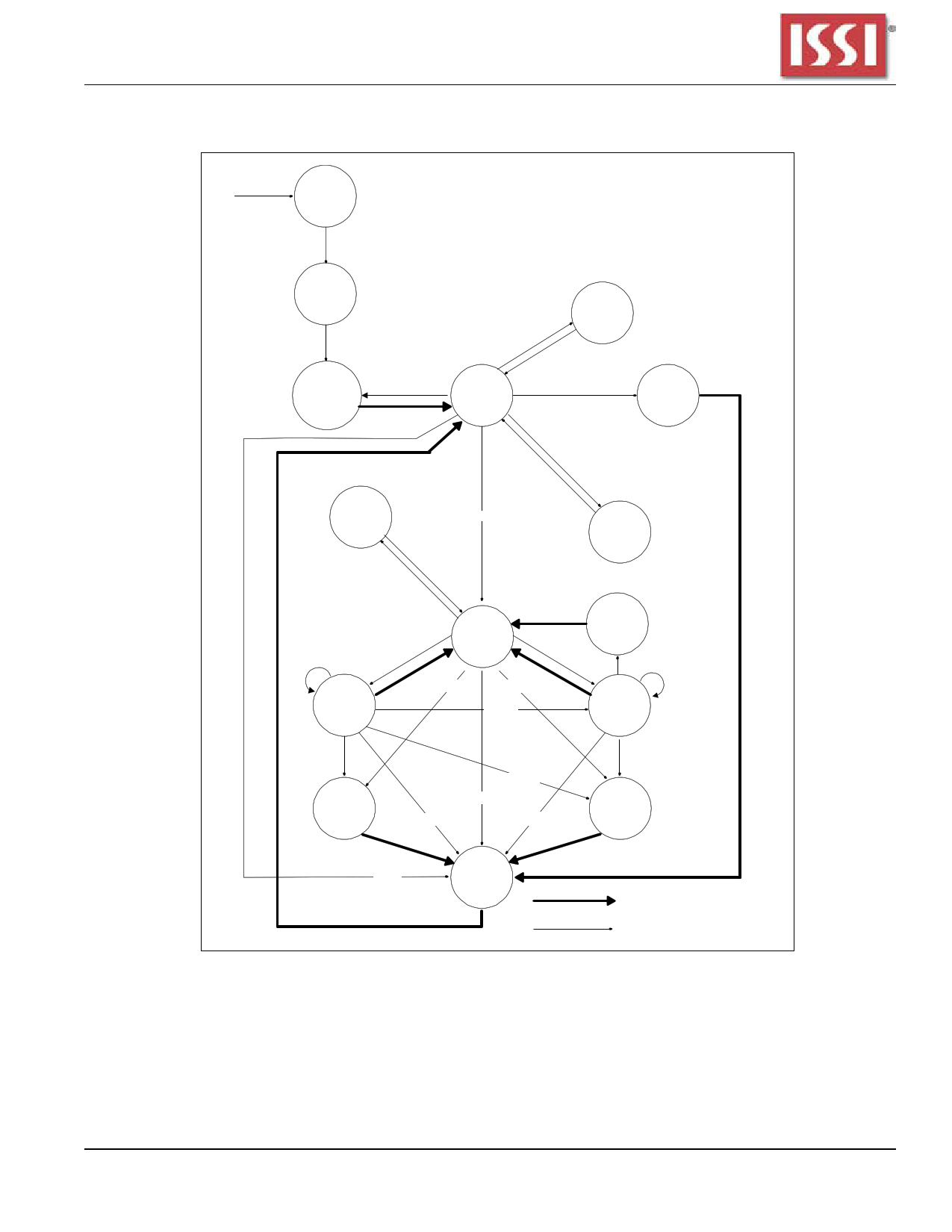
SIMPLIFIED STATE DIAGRAM
Power
Applied
Power
On
Precharge
PREALL
MRS
EMRS
MRS
REFS
Self
Refresh
REFSX
Idle
REFA
Auto
Refresh
CKEH
CKEL
Active
Power
Down
ACT
CKEL
CKEH
Precharge
Power
Down
Write
Write
Write
Row
Active
Read
Burst Stop
Write A
Read A
Read
Read
Read
Write A
Write
A
PRE
PRE
Read
A
PRE
Read A
Read
A
PRE
Precharge
PREALL
Automatic Sequence
Command Sequence
PREALL = Precharge All Banks
CKEL = Enter Power Down
MRS = Mode Register Set
CKEH = Exit Power Down
EMRS = Extended Mode Register Set
ACT = Active
Integrated Silicon Solution, Inc.
Rev. A
09/07/2011
REFS = Enter Self Refresh
Write A = Write with Autoprecharge
REFSX = Exit Self Refresh
Read A = Read with Autoprecharge
REFA = Auto Refresh
PRE = Precharge
5
5 Page 
IS43R32400D
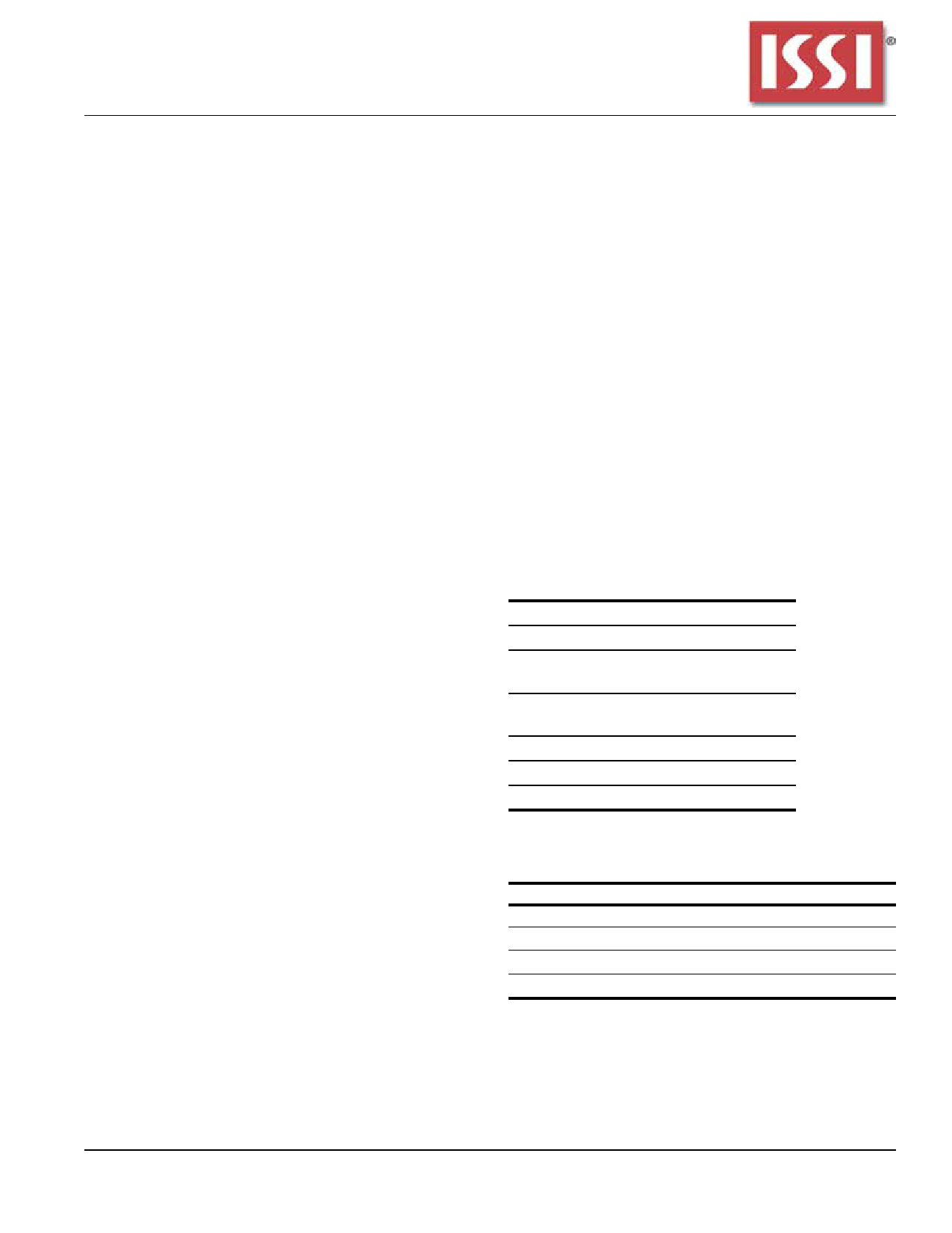
CAS LATENCIES
Integrated Silicon Solution, Inc.
Rev. A
09/07/2011
11
11 Page | ||
| Páginas | Total 30 Páginas | |
| PDF Descargar | [ Datasheet IS43R32400D.PDF ] | |
Hoja de datos destacado
| Número de pieza | Descripción | Fabricantes |
| IS43R32400A | 4Meg x 32 128-MBIT DDR SDRAM | Integrated Silicon Solution |
| IS43R32400D | 128Mb DDR SDRAM | Integrated Silicon Solution |
| IS43R32400E | 128Mb DDR SDRAM | Integrated Silicon Solution |
| Número de pieza | Descripción | Fabricantes |
| SLA6805M | High Voltage 3 phase Motor Driver IC. |
Sanken |
| SDC1742 | 12- and 14-Bit Hybrid Synchro / Resolver-to-Digital Converters. |
Analog Devices |
|
DataSheet.es es una pagina web que funciona como un repositorio de manuales o hoja de datos de muchos de los productos más populares, |
| DataSheet.es | 2020 | Privacy Policy | Contacto | Buscar |
