|
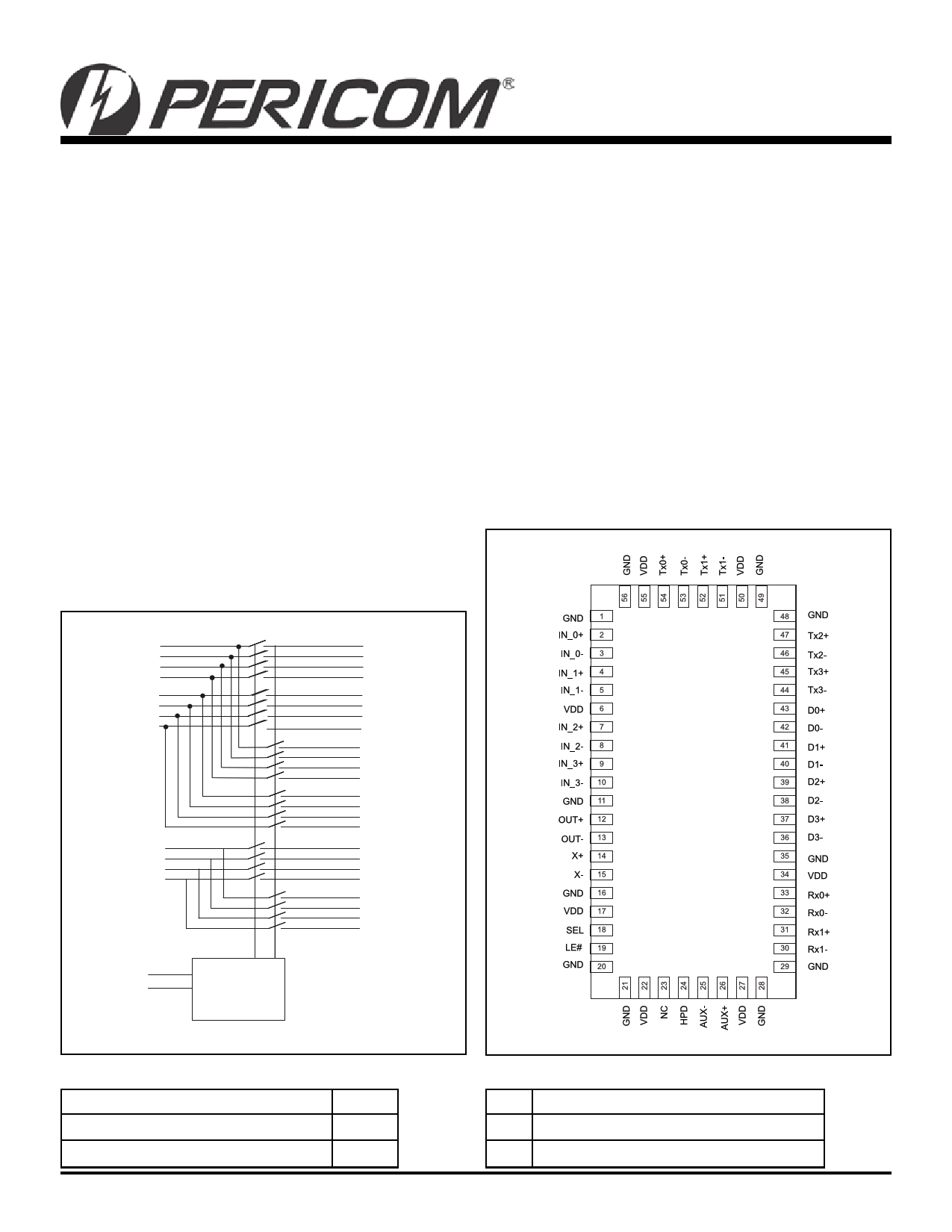
|
|
PDF PI3PCIE2612-A Data sheet ( Hoja de datos )
| Número de pieza | PI3PCIE2612-A | |
| Descripción | 6-Differential Channel 1:2 DP/PCIe Gen2 Display Mux | |
| Fabricantes | Pericom Semiconductor Corporation | |
| Logotipo | ||
Hay una vista previa y un enlace de descarga de PI3PCIE2612-A (archivo pdf) en la parte inferior de esta página. Total 18 Páginas | ||
|
No Preview Available !
PI3PCIE2612-A
High Bandwidth, 6-Differential Channel
1:2 DP/PCIe Gen2 Display Mux, ATX Pinout
Features
• 6 Differential Channel, 1 to 2 demux that will support
5.0Gbps PCIexpress Gen2 signals on one path, and DP 1.1
signals on the second path
• Insertion Loss for high speed channels @ 5.0 Gbps: -5.0dB
• Low Bit-to-Bit Skew , 7ps max (between '+' and '-' bits)
• Latched Mux Select
• Matched paths for all PCIe signals
• Low Crosstalk for high speed channels: [email protected] GHz
• Low Off Isolation for high speed channels: [email protected] GHz
• VDD Operating Range: 3.3V ± 10%
• ESD Tolerance: 8kV HBM on Display Port Path output
3kV HBM on PCI-Express path output
• Low channel-to-channel skew, 35ps max
• Packaging (Pb-free & Green):
– 56 TQFN (ZFE)
Description
Pericom Semiconductor’s PI3PCIE2612-A one to two Mux/
Demux is targeted for next generation systems that combine PCI-
Express gen-II signals with Display Port Signals.
Application
Routing DP and PCIExpress Gen1 or Gen2 signals with low signal
attenuation.
Pin Diagram (top-side view)
Block Diagram
IN_0+
IN_0-
IN_1+
IN_1-
IN_2+
IN_2-
IN_3+
IN_3-
OUT+
OUT-
X+
X-
SEL
LE#
Logic
Control
D0+
D0-
D1+
D1-
D2+
D2-
D3+
D3-
Tx0+
Tx0 -
Tx1+
Tx1 -
Tx2+
Tx2-
Tx3+
Tx3-
AUX+
AUX-
HPD
NC
Rx0+
Rx0-
Rx1+
Rx1-
Truth Table (SEL control)
Function
PCI-Express Gen2 path is active (Tx)
Digital Video Port is active (Dx)
08-0145
SEL
L
H
Truth Table (Latch control)
LE# Internal mux select
0 Respond to changes on SEL
1 Latched
1 PS8925D
07/31/08
1 page 
PI3PCIE2612-A
High Bandwidth, 6-Differential Channel
1:2 DP/PCIe Gen2 Display Mux, ATX Pinout
Maximum Ratings
(Above which useful life may be impaired. For user guidelines, not tested.)
Storage Temperature .....................................................–65°C to +150°C
Supply Voltage to Ground Potential ................................–0.5V to +4.6V
DC Input Voltage ............................................................... –0.5V to VDD
DC Output Current ....................................................................... 120mA
Power Dissipation ............................................................................ 0.5W
Note: Stresses greater than those listed under MAXIMUM
RATINGS may cause permanent damage to the device. This
is a stress rating only and functional operation of the device
at these or any other conditions above those indicated in the
operational sections of this specification is not implied. Expo-
sure to absolute maximum rating conditions for extended
periods may affect reliability.
Electrical Characteristics
Recommended Operating Conditions
Symbol
Parameter
VDD 3.3V Power Supply
Conditions
IDD
TCASE
Total current from
VDD 3.3V supply
Case temperature
range for operation
within spec.
DC Electrical Characteristics (TA = –40°C to +85°C, VDD = 3.3V ± 10%)
Parameter
Description
Test Conditions
VIH-EN(2)
Input high level
VIL-EN(2)
Input Low Level
IIN_EN(2)
Input Leakage Current Measured with input at VIH-EN
max and VIL-EN min
RON On Resistance
VDD = Min., VIN = 1.3V, IIN = 40mA
CON On Channel Capacitance VIN = 0, VDD = 3.3V
Note:
1. Typical values are at VDD = 3.3V, Ta = 25°C ambient and maximum loading.
2. For SEL and LE# inputs
Min Typ Max Units
3.0 3.3 3.6 V
0 2.5 mA
-40 85 Celcius
Min Typ(1) Max
2.0 3.6
Units
V
0 0.8 V
–10 10 uA
10 Ohm
3.0 pF
08-0145
5
PS8925D
07/31/08
5 Page 
Test Circuit for Electrical Characteristics(1-5)
VDD
2 x VDD
Pulse
Generator
VIN
RT
D.U.T
VOUT
200-ohm
4pF
CL
200-ohm
PI3PCIE2612-A
High Bandwidth, 6-Differential Channel
1:2 DP/PCIe Gen2 Display Mux, ATX Pinout
Switch Positions
Test
tPLZ, tPZL
tPHZ, tPZH
Prop Delay
Switch
2 x VDD
GND
Open
Notes:
1. CL = Load capacitance: includes jig and probe capacitance.
2. RT = Termination resistance: should be equal to ZOUT of the Pulse Generator
3. Output 1 is for an output with internal conditions such that the output is low except when disabled by the output control.
output 2 is for an output with internal conditions such that the output is high except when disabled by the output control.
4. All input impulses are supplied by generators having the following characteristics: PRR ≤ MHz, ZO = 50Ω, tR ≤ 2.5ns, tF ≤ 2.5ns.
5. The outputs are measured one at a time with one transition per measurement.
Switching Waveforms
SEL
tPZL
Output 1
tPZH
Output 2
VDD/2
tPLZ
VDD/2
tPHZ
VDD/2
VDD/2
VOL + 0.15V
VOH – 0.15V
VDD
0V
VOH
VOL
VOH
VOL
Voltage Waveforms Enable and Disable Times
08-0145
11
PS8925D
07/31/08
11 Page | ||
| Páginas | Total 18 Páginas | |
| PDF Descargar | [ Datasheet PI3PCIE2612-A.PDF ] | |
Hoja de datos destacado
| Número de pieza | Descripción | Fabricantes |
| PI3PCIE2612-A | 6-Differential Channel 1:2 DP/PCIe Gen2 Display Mux | Pericom Semiconductor Corporation |
| Número de pieza | Descripción | Fabricantes |
| SLA6805M | High Voltage 3 phase Motor Driver IC. |
Sanken |
| SDC1742 | 12- and 14-Bit Hybrid Synchro / Resolver-to-Digital Converters. |
Analog Devices |
|
DataSheet.es es una pagina web que funciona como un repositorio de manuales o hoja de datos de muchos de los productos más populares, |
| DataSheet.es | 2020 | Privacy Policy | Contacto | Buscar |