|
|
|
PDF AD9234 Data sheet ( Hoja de datos )
| Número de pieza | AD9234 | |
| Descripción | Dual Analog-to-Digital Converter | |
| Fabricantes | Analog Devices | |
| Logotipo | ||
Hay una vista previa y un enlace de descarga de AD9234 (archivo pdf) en la parte inferior de esta página. Total 30 Páginas | ||
|
No Preview Available !
Data Sheet
12-Bit, 1 GSPS/500 MSPS JESD204B,
Dual Analog-to-Digital Converter
AD9234
FEATURES
JESD204B (Subclass 1) coded serial digital outputs
1.5 W total power per channel at 1 GSPS (default settings)
SFDR
79 dBFS at 340 MHz (1 GSPS)
86 dBFS at 340 MHz (500 MSPS)
SNR
63.4 dBFS at 340 MHz (AIN = −1.0 dBFS, 1 GSPS)
65.6 dBFS at 340 MHz (AIN = −1.0 dBFS, 500 MSPS)
ENOB = 10.4 bits at 10 MHz
DNL = ±0.16 LSB; INL = ±0.35 LSB
Noise density
−151 dBFS/Hz (1 GSPS)
−150 dBFS/Hz (500 MSPS)
1.25 V, 2.5 V, and 3.3 V dc supply operation
Low swing full scale input
1.34 V p-p nominal (1 GSPS)
1.63 V p-p nominal (500 MSPS)
No missing codes
Internal ADC voltage reference
Flexible termination impedance
400 Ω, 200 Ω, 100 Ω, and 50 Ω differential
2 GHz usable analog input full power bandwidth
95 dB channel isolation/crosstalk
Amplitude detect bits for efficient AGC implementation
Differential clock input
Optional decimate-by-2 DDC per channel
Differential clock input
Integer clock divide by 1, 2, 4, or 8
Flexible JESD204B lane configurations
Small signal dither
APPLICATIONS
Communications
Diversity multiband, multimode digital receivers
3G/4G, TD-SCDMA, W-CDMA, GSM, LTE
Point-to-point radio systems
Digital predistortion observation path
General-purpose software radios
Ultrawideband satellite receiver
Instrumentation (spectrum analyzers, network analyzers,
integrated RF test solutions)
Digital oscilloscopes
High speed data acquisition systems
DOCSIS 3.0 CMTS upstream receive paths
HFC digital reverse path receivers
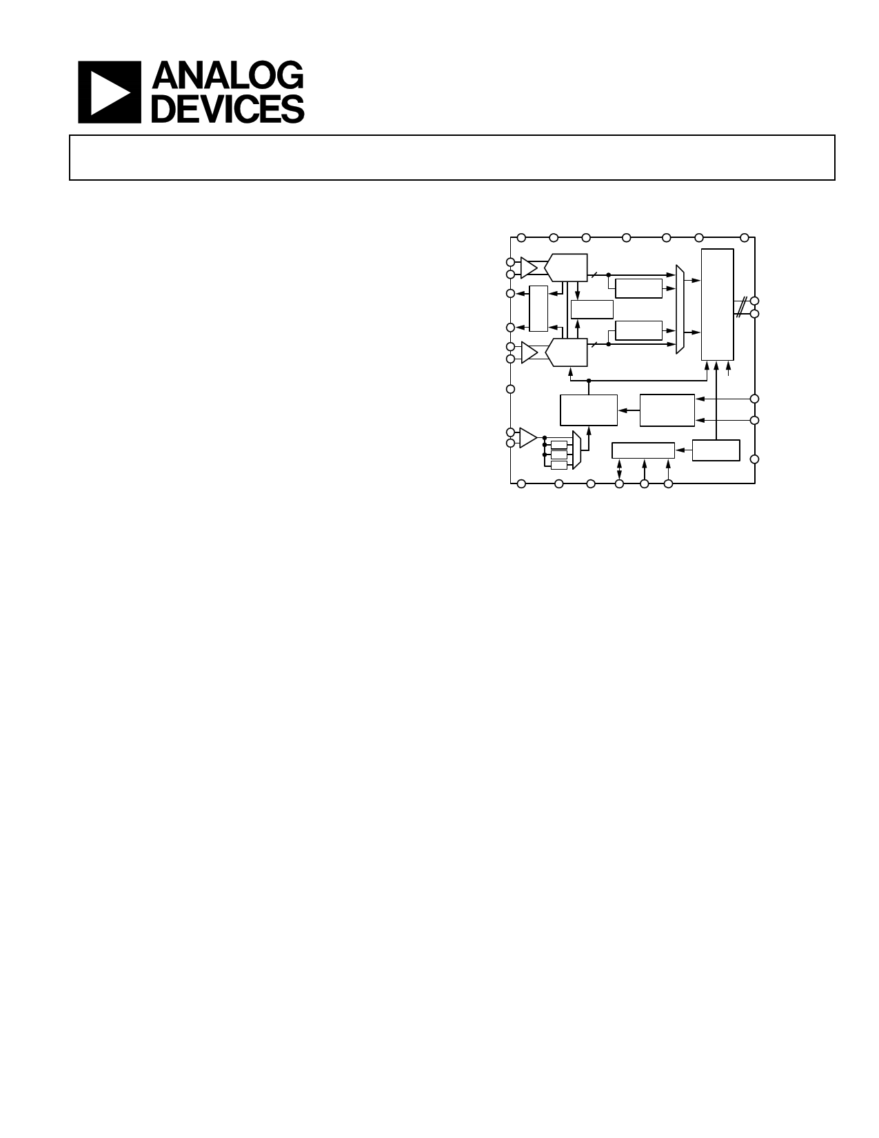
FUNCTIONAL BLOCK DIAGRAM
AVDD1 AVDD2 AVDD3 AVDD1_SR DVDD DRVDD SPIVDD
(1.25V) (2.5V) (3.3V) (1.25V) (1.25V) (1.25V) (1.8V TO 3.3V)
VIN+A
VIN–A
FD_A
FD_B
VIN+B
VIN–B
V_1P0
CLK+
CLK–
BUFFER
ADC
CORE 12
DECIMATE
BY 2
SIGNAL
MONITOR
12
ADC
CORE
DECIMATE
BY 2
BUFFER
CLOCK
GENERATION
AND ADJUST
JESD204B
SUBCLASS 1
CONTROL
4 SERDOUT0±
SERDOUT1±
SERDOUT2±
SERDOUT3±
FAST
DETECT
SYNCINB±
SYSREF±
÷2
÷4
SPI CONTROL
SIGNAL
MONITOR
PDWN/
÷8
AD9234
STBY
AGND DRGND DGND SDIO SCLK CSB
Figure 1.
PRODUCT HIGHLIGHTS
1. Low power consumption analog core, 12-bit, 1.0 GSPS dual
analog-to-digital converter (ADC) with 1.5 W per channel.
2. Wide full power bandwidth supports IF sampling of signals
up to 2 GHz.
3. Buffered inputs with programmable input termination
eases filter design and implementation.
4. Flexible serial port interface (SPI) controls various product
features and functions to meet specific system requirements.
5. Programmable fast overrange detection.
6. 9 mm × 9 mm 64-lead LFCSP.
7. Pin compatible with the AD9680 14-bit, 1 GSPS/500 MSPS
dual ADC.
Rev. A
Document Feedback
Information furnished by Analog Devices is believed to be accurate and reliable. However, no
responsibilityisassumedbyAnalogDevices for itsuse,nor foranyinfringementsofpatentsor other
rights of third parties that may result from its use. Specifications subject to change without notice. No
license is granted by implication or otherwise under any patent or patent rights of Analog Devices.
Trademarksandregisteredtrademarksarethepropertyoftheirrespectiveowners.
One Technology Way, P.O. Box 9106, Norwood, MA 02062-9106, U.S.A.
Tel: 781.329.4700 ©2014–2015 Analog Devices, Inc. All rights reserved.
Technical Support
www.analog.com
1 page 
Data Sheet
AD9234
SPECIFICATIONS
DC SPECIFICATIONS
AVDD1 = 1.25 V, AVDD2 = 2.5 V, AVDD3 = 3.3 V, AVDD1_SR = 1.25 V, DVDD = 1.25 V, DRVDD = 1.25 V, SPIVDD = 1.8 V, specified
maximum sampling rate, AIN = −1.0 dBFS, clock divider = 2, default SPI settings, TA = 25°C, unless otherwise noted.
Table 1.
Parameter
RESOLUTION
ACCURACY
No Missing Codes
Offset Error
Offset Matching
Gain Error
Gain Matching
Differential Nonlinearity (DNL)
Integral Nonlinearity (INL)
TEMPERATURE DRIFT
Offset Error
Gain Error
INTERNAL VOLTAGE REFERENCE
Voltage
INPUT-REFERRED NOISE
VREF = 1.0 V
ANALOG INPUTS
Differential Input Voltage Range
Common-Mode Voltage (VCM)
Differential Input Capacitance1
Analog Input Full Power Bandwidth
POWER SUPPLY
AVDD1
AVDD2
AVDD3
AVDD1_SR
DVDD
DRVDD
SPIVDD
IAVDD1
IAVDD2
IAVDD3
IAVDD1_SR
IDVDD2
IDRVDD1
IDRVDD (L = 2 mode)
ISPIVDD
Temp
Full
AD9234-500
Min Typ Max
12
AD9234-1000
Min Typ Max
12
Unit
Bits
Full Guaranteed
Guaranteed
Full −0.22 0 +0.20 −0.22 0
+0.20 % FSR
Full
0 +0.19
0 +0.19 % FSR
Full −13.8 −5.1 +3.6
0
% FSR
Full −3.9 +1 +5.9
1 +4.8 % FSR
Full −0.3
+0.3 −0.3 ±0.16 +0.3 LSB
Full −0.8
+1.1 −1.2 ±35
+1.4 LSB
25°C ±2.6
25°C ±36
±6 ppm/°C
±36 ppm/°C
Full 1.0
1.0 V
25°C 0.74
1.02 LSB rms
Full 1.63
25°C 2.05
25°C 1.5
25°C 2
1.34 V p-p
2.05 V
1.5 pF
2 GHz
Full 1.22 1.25 1.28 1.22 1.25 1.28 V
Full 2.44 2.50 2.56 2.44 2.50 2.56 V
Full 3.2 3.3 3.4 3.2 3.3 3.4 V
Full 1.22 1.25 1.28 1.22 1.25 1.28 V
Full 1.22 1.25 1.28 1.22 1.25 1.28 V
Full 1.22 1.25 1.28 1.22 1.25 1.28 V
Full 1.7 1.8 3.4 1.7 1.8 3.4 V
Full 430 480 675 740 mA
Full 380 430 525 590 mA
Full 65 75
75 91 mA
Full 15 18
16 18 mA
Full 140 152 230 236 mA
Full 190 246 205 225 mA
25°C 140
N/A3
mA
Full 5 6
5 6 mA
Rev. A | Page 5 of 66
5 Page 
Data Sheet
ABSOLUTE MAXIMUM RATINGS
Table 6.
Parameter
Electrical
AVDD1 to AGND
AVDD1_SR to AGND
AVDD2 to AGND
AVDD3 to AGND
DVDD to DGND
DRVDD to DRGND
SPIVDD to AGND
AGND to DRGND
VIN±x to AGND
SCLK, SDIO, CSB to AGND
PDWN/STBY to AGND
Operating Temperature Range
Junction Temperature Range
Storage Temperature Range (Ambient)
Rating
1.32 V
1.32 V
2.75 V
3.63 V
1.32 V
1.32 V
3.63 V
−0.3 V to +0.3 V
3.2 V
−0.3 V to SPIVDD + 0.3 V
−0.3 V to SPIVDD + 0.3 V
−40°C to +85°C
−40°C to +115°C
−65°C to +150°C
Stresses at or above those listed under Absolute Maximum
Ratings may cause permanent damage to the product. This is a
stress rating only; functional operation of the product at these
or any other conditions above those indicated in the operational
section of this specification is not implied. Operation beyond
the maximum operating conditions for extended periods may
affect product reliability.
AD9234
THERMAL CHARACTERISTICS
Typical θJA, θJB, and θJC are specified vs. the number of printed
circuit board (PCB) layers in different airflow velocities (in
m/sec). Airflow increases heat dissipation effectively reducing
θJA and θJB. In addition, metal in direct contact with the package
leads and exposed pad from metal traces, through holes, ground,
and power planes, reduces the θJA. Thermal performance for
actual applications requires careful inspection of the conditions
in an application. The use of appropriate thermal management
techniques is recommended to ensure that the maximum
junction temperature does not exceed the limits shown in Table 6.
Table 7. Thermal Resistance Values
PCB
Type
Airflow
Velocity
(m/sec) θJA
ΨJB
JEDEC
2s2p
Board
0.0
1.0
2.5
17.81, 2
15.61, 2
15.01, 2
6.31, 3
5.91, 3
5.71, 3
θJC_TOP
4.71, 5
N/A4
N/A4
θJC_BOT
1.21, 5
Unit
°C/W
°C/W
°C/W
1 Per JEDEC 51-7, plus JEDEC 51-5 2s2p test board.
2 Per JEDEC JESD51-2 (still air) or JEDEC JESD51-6 (moving air).
3 Per JEDEC JESD51-8 (still air).
4 N/A = not applicable.
5 Per MIL-STD 883, Method 1012.1.
ESD CAUTION
Rev. A | Page 11 of 66
11 Page | ||
| Páginas | Total 30 Páginas | |
| PDF Descargar | [ Datasheet AD9234.PDF ] | |
Hoja de datos destacado
| Número de pieza | Descripción | Fabricantes |
| AD9230 | 1.8 V Analog-to-Digital Converter | Analog Devices |
| AD9233 | Analog-to-Digital Converter | Analog Devices |
| AD9234 | Dual Analog-to-Digital Converter | Analog Devices |
| AD9235 | 3V A/D Converter | Analog Devices |
| Número de pieza | Descripción | Fabricantes |
| SLA6805M | High Voltage 3 phase Motor Driver IC. |
Sanken |
| SDC1742 | 12- and 14-Bit Hybrid Synchro / Resolver-to-Digital Converters. |
Analog Devices |
|
DataSheet.es es una pagina web que funciona como un repositorio de manuales o hoja de datos de muchos de los productos más populares, |
| DataSheet.es | 2020 | Privacy Policy | Contacto | Buscar |