|
|
PDF IS46LR32640A Data sheet ( Hoja de datos )
| Número de pieza | IS46LR32640A | |
| Descripción | 16M x 32Bits x 4Banks Mobile DDR SDRAM | |
| Fabricantes | ISSI | |
| Logotipo |  |
|
Hay una vista previa y un enlace de descarga de IS46LR32640A (archivo pdf) en la parte inferior de esta página. Total 30 Páginas | ||
|
No Preview Available !
IS43/46LR32640A
16M x 32Bits x 4Banks Mobile DDR SDRAM
Description
The IS43/46LR32640A is 2,147,483,648 bits CMOS Mobile Double Data Rate Synchronous DRAM organized as 4 banks of 33,554,432 words
x 32 bits. This product uses a double-data-rate architecture to achieve high-speed operation. The Data Input/ Output signals are transmitted
on a 32-bit bus. The double data rate architecture is essentially a 2N prefetch architecture with an interface designed to transfer two data
words per clock cycle at the I/O pins. This product offers fully synchronous operations referenced to both rising and falling edges of the clock.
The data paths are internally pipelined and 2n-bits prefetched to achieve very high bandwidth. All input and output voltage levels are
compatible with LVCMOS.
Features
• JEDEC standard 1.8V power supply.
• VDD = 1.8V, VDDQ = 1.8V
• Four internal banks for concurrent operation
• MRS cycle with address key programs
- CAS latency 2, 3 (clock)
- Burst length (2, 4, 8)
- Burst type (sequential & interleave)
• Fully differential clock inputs (CK, /CK)
• All inputs except data & DM are sampled at the rising
edge of the system clock
• Data I/O transaction on both edges of data strobe
• Bidirectional data strobe per byte of data (DQS)
• DM for write masking only
• Edge aligned data & data strobe output
• Center aligned data & data strobe input
• 64ms refresh period (8K cycle)
• Auto & self refresh
• Concurrent Auto Precharge
• Maximum clock frequency up to 200MHZ
• Maximum data rate up to 400Mbps/pin
• Power Saving support
- PASR (Partial Array Self Refresh)
- Auto TCSR (Temperature Compensated Self Refresh)
- Deep Power Down Mode
- Programmable Driver Strength Control by Full Strength
or 1/2, 1/4, or 1/8 of Full Strength
• LVCMOS compatible inputs/outputs
• 90-Ball FBGA package
• 64Mx32 (two stacked 16Mx16x4 banks)
Copyright © 2014 Integrated Silicon Solution, Inc. All rights reserved. ISSI reserves the right to make changes to this specification and its
products at any time without notice. ISSI assumes no liability arising out of the application or use of any information, products or services
described herein. Customers are advised to obtain the latest version of this device specification before relying on any published information
and before placing orders for products.
Integrated Silicon Solution, Inc. does not recommend the use of any of its products in life support applications where the failure or
malfunction of the product can reasonably be expected to cause failure of the life support system or to significantly affect its safety or
effectiveness. Products are not authorized for use in such applications unless Integrated Silicon Solution, Inc. receives written assurance to
its satisfaction, that:
a.) the risk of injury or damage has been minimized;
b.) the user assume all such risks; and
c.) potential liability of Integrated Silicon Solution, Inc is adequately protected under the circumstances
Rev. A | Feb 2014
www.issi.com - [email protected]
1
1 page 
IS43/46LR32640A
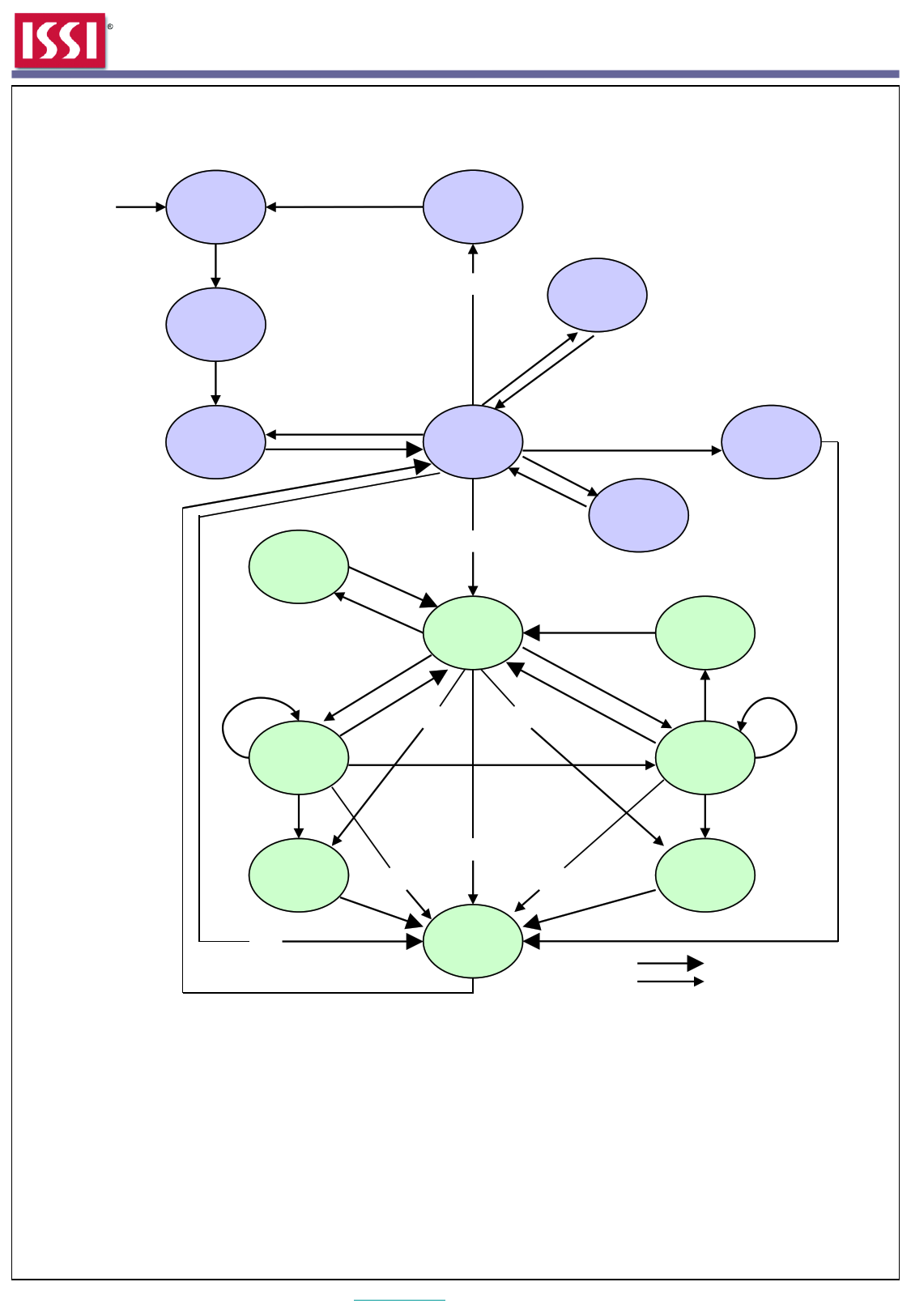
Figure3 : Simplified State Diagram
Power
Applied
Power
On
DPDSX
Deep Power
Down
Precharge
All Banks
DPDS
Self
Refresh
REFS
REFSX
MRS
EMRS
MRS
Active
Power
Down
CKEH
Idle
All Banks
Precharged
CKEL
REFA
CKEH
ACT
Precharge
Power
Down
Auto
Refresh
CKEL
Row
Active
Burst
Stop
WRITE
WRITE
WRITE
WRITE A READ A
READ
READ
BST
READ
READ
WRITE A
WRITE A
PRE
PRE
PRE
PRE
Precharge
PREALL
READ A
READ A
Automatic
sequence
Rev. A | Feb 2014
ACT = Active
BST = Burst
CKEL = Enter Power- Down
CKEH = Exit Power-Down
DPDS = Enter Deep Power-Down
DPDSX = Exit Deep Power- Down
EMRS = Ext. Mode Reg. Set
MRS = Mode Register Set
PRE = Precharge
PREALL= Precharge All Banks
REFA = Auto Refresh
REFS = Enter Self Refresh
REFSX = Exit Self Refresh
READ = Read w/o Auto Precharge
READ A = Read with Auto Precharge
WRITE = Write w/o Auto Precharge
WRITE A = Write with Auto Precharge
www.issi.com - [email protected]
5
5 Page 
IS43/46LR32640A
Mode Register
The mode register is used to define the specific mode of operation of the Mobile DDR SDRAM. This definition includes the selection of a
burst length, a burst type, a CAS latency. The mode register is programmed via the LOAD MODE REGISTER command and will retain the
stored information until programmed again, the device goes into deep power-down mode, or the device loses power.
Mode register bits A0-A2 specify the burst length, A3 specifies the type of burst (sequential or interleaved), A4-A6 specify the CAS latency,
and A7-A13 should be set to zero. BA0 and BA1 must be zero to access the mode register.
The mode register must be loaded when all banks are idle, and the controller must wait the specified time before initiating the subsequent
operation. Violating either of these requirements will result in unspecified operation.
Burst Length
Read and write accesses to the Mobile DDR SDRAM are burst oriented, with the burst length being programmable, as shown in Figure
(Mode Register Set Definition). The burst length determines the maximum number of column locations that can be accessed for a given
READ or WRITE command. Burst lengths of 2, 4, or 8 are available for both the sequential and the interleaved burst types.
Reserved states should not be used, as unknown operation or incompatibility with future versions may result. When a READ or WRITE
command is issued, a block of columns equal to the burst length is effectively selected. All accesses for that burst take place within this
block, meaning that the burst will wrap within the block if a boundary is reached. The block is uniquely selected by A1-A9 when the burst
length is set to two; by A2-A9 when the burst length is set to four; by A3-A9 when the burst length is set to eight; and by A4-A9 when the
burst length is set to sixteen. The remaining (least significant) address bit(s) is (are) used to select the starting location within the block.
The programmed burst length applies to both READ and WRITE bursts.
CAS Latency
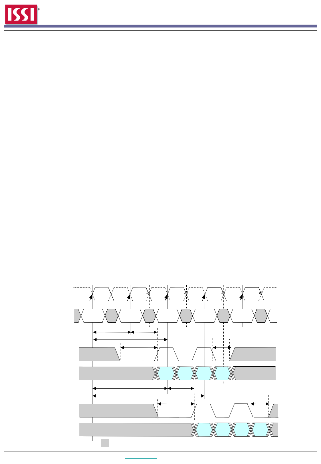
The CAS latency is the delay, in clock cycles, between the registration of a READ command and the availability of the first bit of output
data. The latency can be set to 2, 3 clocks, as shown in Figure (Standard Mode Register Definition).
For CL = 3, if the READ command is registered at clock edge n, then the data will be available at (n + 2 clocks + tAC). For CL = 2, if the
READ command is registered at clock edge n, then the data will be available at (n + 1 clock + tAC).
Figure7 : CAS Latency (BL=4)
/C LK
CLK
T0
T1 T1n T2 T2n T3 T3n T4 T4n
Command
READ
NOP
NOP
NOP
NOP
DQS
1tCK
tAC
CL = 2
tRPRE
tRPST
DQ
DQS
2tCK
CL = 3
D OUT
n
D OUT
n+1
tAC
D OUT
n+2
D OUT
n+3
tRPRE
tRPST
DQ
Rev. A | Feb 2014
Don ’t care
D OUT
n
www.issi.com - [email protected]
DOUT
n+1
D OUT
n+2
DOUT
n+3
11
11 Page | ||
| Páginas | Total 30 Páginas | |
| PDF Descargar | [ Datasheet IS46LR32640A.PDF ] | |
Hoja de datos destacado
| Número de pieza | Descripción | Fabricantes |
| IS46LR32640A | 16M x 32Bits x 4Banks Mobile DDR SDRAM | ISSI |
| Número de pieza | Descripción | Fabricantes |
| SLA6805M | High Voltage 3 phase Motor Driver IC. |
Sanken |
| SDC1742 | 12- and 14-Bit Hybrid Synchro / Resolver-to-Digital Converters. |
Analog Devices |
|
DataSheet.es es una pagina web que funciona como un repositorio de manuales o hoja de datos de muchos de los productos más populares, |
| DataSheet.es | 2020 | Privacy Policy | Contacto | Buscar |
